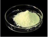
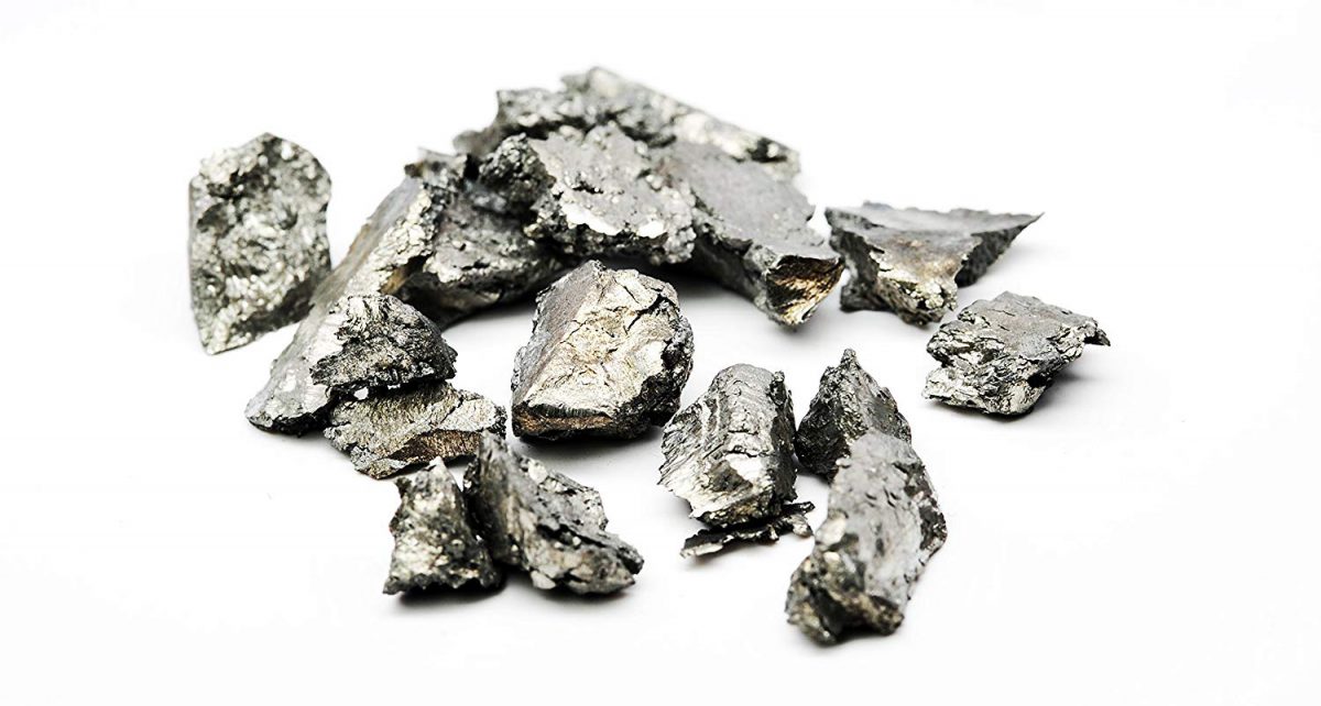
Holmium oxide is a chemical compound of rare-earth element holmium and oxygen with the formula Ho2O3. Together with dysprosium oxide, it is considered one of the most paramagnetic substances known. Holmium oxide is one of the constituents of erbium oxide minerals. In the natural state, holmium oxide often coexists with trivalent oxides of lanthanides, and we need special methods to separate them. Holmium oxide can be used to prepare a glass of a particular color. The visible absorption spectrum of Ho2O3-containing glasses and solutions has a series of sharp peaks and is therefore traditionally used as a standard for spectroscopic calibration.
Properties
Appearance
Light yellow or yellow powder, belonging to the equiaxed crystal yttria type structure
Density (g/mL, 25 ° C)
8.16
Melting point (° C)
2415
Boiling point (° C, atmospheric pressure)
3900
Solubility
insoluble in water, soluble in acid
Chemical reaction
Ho2O3+ 6 NH4Cl → 2 HoCl3+ 6 NH3+ 3 H2O
Applications
It is used to manufacture new light source xenon lamps, and can also be used as an additive for yttrium iron obtained from yttrium aluminum garnet and to prepare metal holmium. Holmium oxide can be used as a yellow and red colorant for Soviet diamonds and glass. Glass containing holmium oxide and holmium oxide solution (often perchloric acid solution) have sharp absorption peaks in the spectrum of 200-900 nm, and thus can be used as a standard for spectrometer calibration and have been commercialized. Like other rare earth elements, cerium oxide is also used as a special catalyst, phosphor, laser and coating material (sputtering targets & evaporation materials).
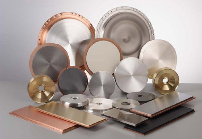
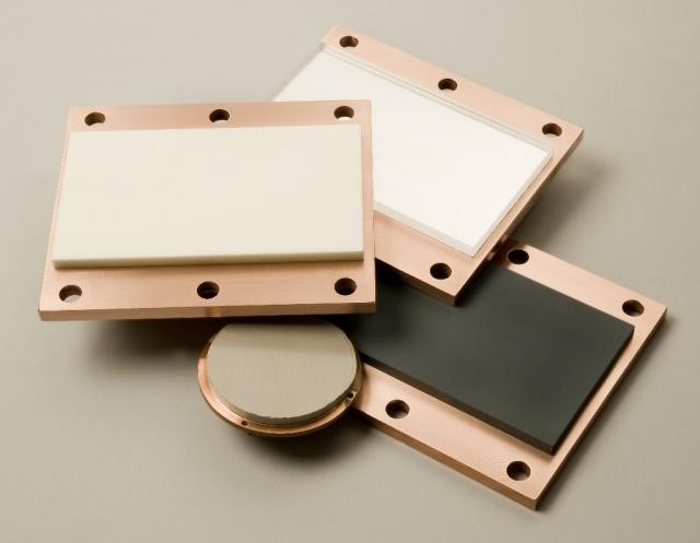
Holmium oxide sputtering targets
Holmium oxide sputtering targets with the highest quality can be used in semiconductor, chemical vapor deposition (CVD) and physical vapor deposition (PVD) applications. Stanford Advanced Materials (SAM) Sputtering Target Manufacturer offers target bonding service, reclaim service and customized service, which can help you make full use of the coating materials.
Rare earth oxides (REOs) have gained more and more attention due to their unique magnetic, luminescent, and electrochemical properties. They are used for applications in various industries such as nuclear, electronics, lasers, and etc. Among them, although Gadolinium oxide (Gd2O3) is not the most widely used REOs, but is the most researched one.
The key property of Gadolinium Oxide
Chemical formula
Gd2O3
Molar mass
362.50 g/mol
Magnetic susceptibility
+53,200·10−6 cm3/mol
Density
7.41 (g/cm3)
Melting Point
2330 (°C)
Gadolinium oxide preparation
Gadolinium oxide can be formed by thermal decomposition of the hydroxide, nitrate, carbonate, or oxalates. Specifically, first, use monazite or a mixed rare earth ore as the raw material. Then Extract and purify the ore to prepare the samarium-gadolinium mixed rare earth solution. Use oxalic acid to precipitate gadolinium oxalic acid. Then separate, dry, and burn the gadolinium oxalic acid to obtain gadolinium oxide.
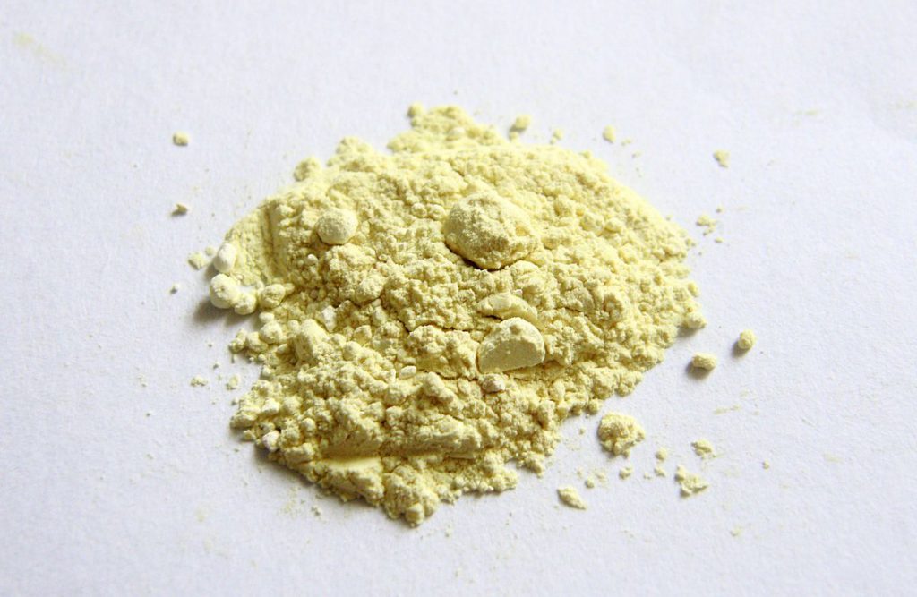
Gadolinium oxide powder
Gadolinium oxide is a white powder. It is insoluble in water but soluble in acid. It easily absorbs moisture and carbon dioxide from the air. It can be used as a raw material for various fluorescent compounds, absorption material in atomic reactions, nuclear fuels, magnetic bubble material, screen-sensitivity increasing material, as well as many other applications in the chemical, glass and electronic industries.
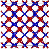
Gadolinium Oxide Structure
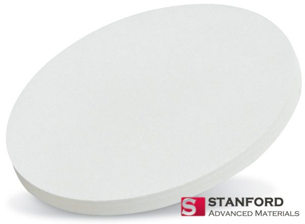
Gadolinium oxide sputtering target
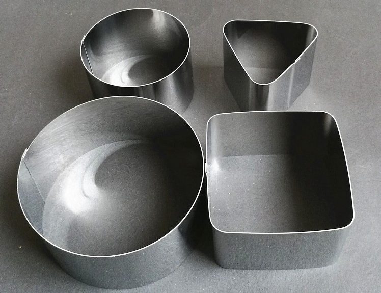
Gadolinium oxide sputtering target is the product made of gadolinium oxide materials by casting or powder metallurgy. Common shapes of the gadolinium oxide sputter targets are planar, circular, rotary, and rectangular. In general, planar targets are cheaper but rotary targets have a higher utilization rate. Gadolinium oxide sputtering target is specially used in the sputtering process (a method of physical vapor deposition) to form a film on the substrate of glass, metal or other materials. Its purpose is either to protect the substrate or improve its properties.
Gadolinium oxide microcrystal
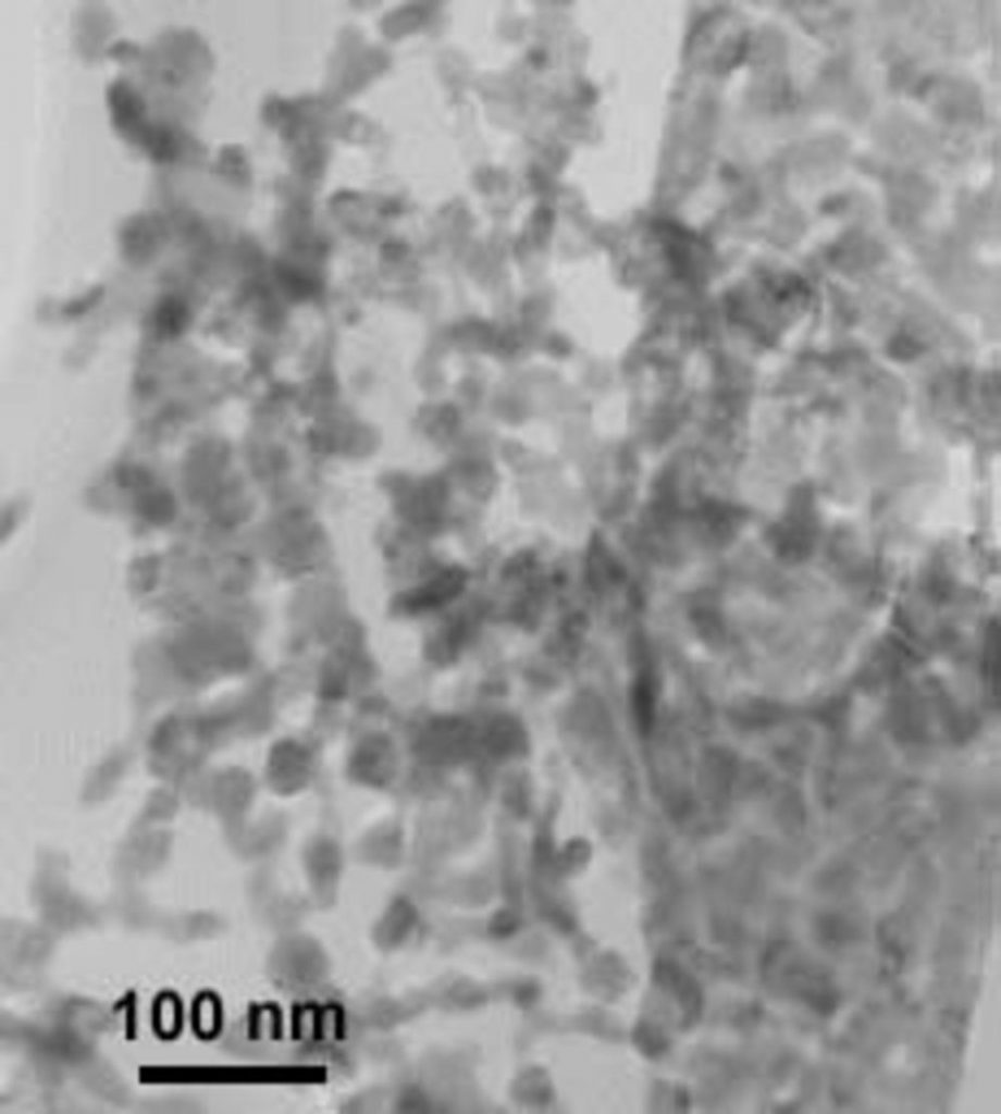
Gadolinium oxide microcrystal is defined as the gadolinium oxide nanomaterial with at least one direction usually in the range of 1–100 nm. These materials have different physical, chemical, and electrical properties in comparison with traditional bulk gadolinium oxide materials. These nanomaterials have the crystallographic stability up to temperatures of 2325°C, high mechanical strength, excellent thermal conductivity, and a wide band optical gap. Thus, they are used for new products and applications and may also be incorporated into various industrial processes in the nuclear industry, electronics, lasers, and optical material.
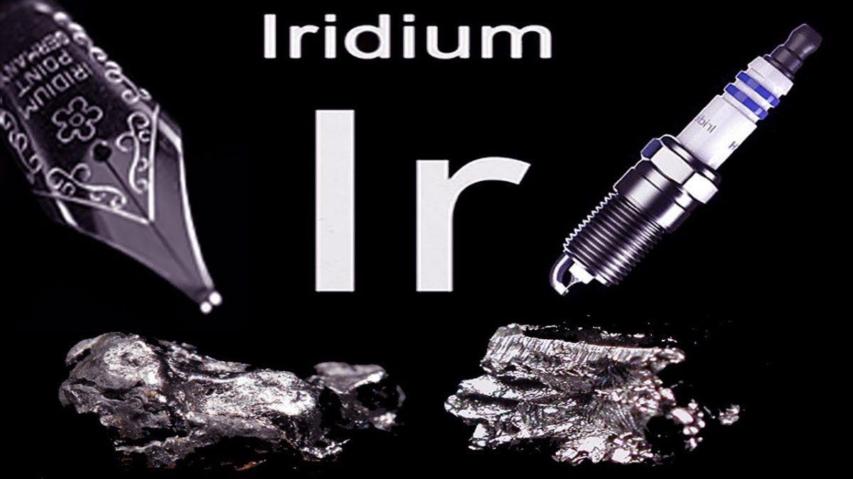
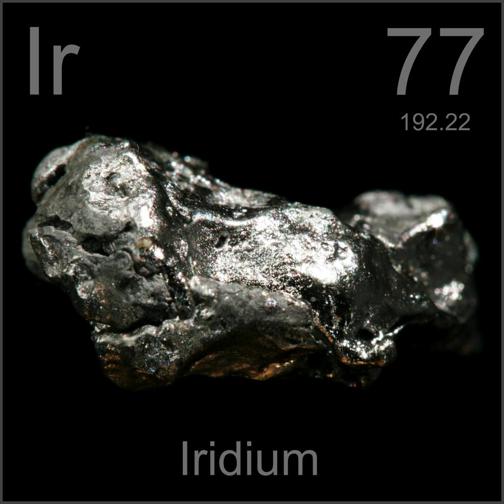
Iridium, a very hard, brittle, silvery-white transition metal of the platinum group, is the second-densest metal (after osmium) with a density of 22.56 g/cm3 as defined by experimental X-ray crystallography.
Discovery
Smithson TennantIridium was discovered together with osmium in1803 by English chemist Smithson Tennant in London. When crude platinum was dissolved in dilute aqua regia (a mixture of nitric and hydrochloric acids), it left behind a black residue. Because of the black color, it was initially thought to be graphite. By treating it alternately with alkalis and acids, Tennant was able to separate it into two new elements. These he announced at the Royal Institution in London, naming one iridium (comeing from the Latin word ‘iris’, meaning rainbow) because many of its salts were so colorful; and the other osmium (derived from osme, the Greek word for smell) because it had a curious odor.
Specification
Name
Iridium
Symbol
Ir
Color
silvery-white
CAS number
7439-88-5
Melting point
2446°C, 4435°F, 2719 K
Boiling point
4428°C, 8002°F, 4701 K
Density (g cm−3)
22.5622
Feature
Iridium is a rare, hard, lustrous, brittle, very dense platinum-like metal. Chemically it is almost as unreactive as gold. It is the most corrosion-resistant metal known and it resists attack by any acid. Iridium is generally credited with being the second densest element (after osmium) based on measured density, although calculations involving the space lattices of the elements show that iridium is denser.
Application
Due to its good corrosion-resistance, it is used of as a hardening agent for special alloy or to form an alloy with osmium, which is used for bearing compass and tipping pens.
Iridium is used in making Iridium crucibles and other equipment that is used at high temperatures. Iridium sputtering target is a coating material to produce Iridium film, which is used as protective film or heavy-duty electrical contacts. In addition, Iridium was used in making the international standard kilogram, which is an alloy of 90% platinum and 10% iridium.
Although the rotary targets have developed in recent years, the mainstream shape of the sputtering target is still the planar type. Today let us take a look at the pros and cons of planar targets to help you determine whether a planar sputtering target is suitable for your project.
Advantages of Planar Sputter Target
Simple structure – one of the main advantages of the planar target is that the structure is simple. The common planar targets on the market are rectangular planar targets and circular planar targets, which are easily produced by molds. In other words, planar target preparation requires fewer machines and technologies and is easier to prepare. This is why planar targets still dominate the sputtering target market.
Molds
Low price – You can never deny that the price is always an important competitive factor. As mentioned above, the manufacturing process of the planar sputter target is easier, so its price is much lower than the rotatory sputter target.
Strong versatility – Planar sputtering targets usually have strong versatility. Therefore, the transportation of the planar targets is relatively simple and is not easily damaged during transportation.
Good uniformity and repeatability – Film layers sputtered by planar targets usually boast good uniformity and repeatability. Planar targets are still best suited for prototype work or elemental experimentation, especially when large amounts of material are not needed at once.
Disadvantages of Planar Sputter Target
Its biggest disadvantage is the low utilization rate (generally only about 20%). In the sputtering process of the planar target, a strip-shaped pit will be formed when the target of the glow region (the magnetic field distribution region) is consumed to a certain extent, making the target body thinner. And once the pit depth reaches a certain value, the target cannot be utilized anymore. The low utilization rate also reduces its price advantage to some extent.
In conclusion, planar targets are still the best choice for prototype work or elemental experimentation, especially when large amounts of material are not needed at once. But its disadvantage of low utilization rate (20% vs. 80% compared with the rotatory target) does constrain its development.
Next week, let us look at the biggest competitor of the planar target– the rotatory target. Weighting the pros and cons of these two types of sputtering target may help you better choose the one for your application.
Evaporation pellets are evaporation materials for vacuum evaporation coating.
Evaporation is a form of physical vapor deposition (PVD) where the evaporation material is heated to a high vapor pressure, often in a molten state. The vapors are then condensed on the substrate to form a thin film.
The most common heating method for vacuum evaporation is the resistance heating method. The advantages of resistance heating method include simple structure, low cost and convenient operation. The disadvantage is that it is not suitable for refractory metals and high temperature resistant dielectric materials. Electron beam heating and laser heating can overcome the shortcomings of resistance heating. Electron beam heating uses a focused electron beam to directly heat the bombarded material, and the kinetic energy of the electron beam becomes thermal energy, causing the material to evaporate. Laser heating uses a high-power laser as a heating source, but due to the high cost of high-power lasers, it can only be used in a few research laboratories. You can refer to Five evaporation sources for heating for detailed information of the heating methods. As for a thin film precious metal coating, the heating is typically accomplished via resistive heating or by E-beam (electron beam).
Evaporation pellets or slugs are manufactured with specific form factors intended to vaporize at known rates. Often during evaporation processes, “spitting” results in liquid droplet material splattering on to the substrate. Engineered pellets are made with specified metal purities and processes intended to minimize incorporated gases and impurities to mitigate “spitting” in process.
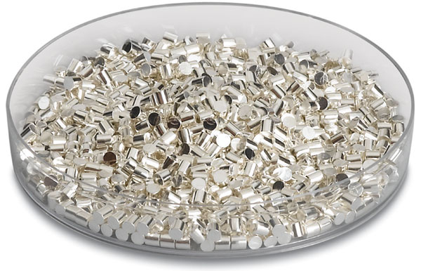
Silver (Ag) Evaporation Materials
Optimal evaporative performance for thin film deposition is highly dependent on the use of high purity materials specifically customized for PVD processes. It requires evaporation materials that feature low organic and inorganic impurities, as well as minimal surface contamination. This level of purity results in highly reproducible performance with low spit rates and defects. SAM offers high-quality evaporation materials in precious metals for your PVD coating.
The following chart shows some common thin film deposition of precious metals. SAM can customize any precious metal alloy you need that is not listed.
Yttrium is a silvery-metallic transition metal chemically similar to the lanthanides and has often been classified as a “rare-earth element“. Yttrium was discovered as early as the 18th century, but it has not been widely used until the last few decades in chemistry, physics, computer technology, film coating, medicine and other fields.
Yttrium History
In 1787, while the Swedish chemist Carl Axel Arrhenius exploring a quarry near Ytterby, a small town near Sweden’s capital city, Stockholm, he discovered an unusual black rock. He thought that he had discovered a new mineral, and sent some specimens to Johan Gadolin, a Finnish mineralogist, for analysis.
During the analysis, Gadolin isolated the yttrium from the mineral. The mineral was later named gadolinite in Gadolin’s honor, and Yttrium was named Ytterby from where the mineral was discovered.
In 1843, a Swedish chemist named Carl Gustaf Mosander studied yttrium samples and discovered three oxides, which were called yttria, erbia and terbia at that time. Currently, they are known as yttrium oxide (white), terbium oxide (yellow), and erbium oxide (rose-colored). A fourth oxide, ytterbium oxide, was identified in 1878.
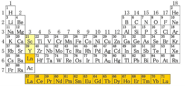
Yttrium, a transition metal
In the Periodic Table of Elements, yttrium is considered one of the transition metals (yellow in the pic). Other more well-known transition metal elements include gold, silver and iron. The transition metals are the metallic elements that serve as a bridge, or transition, between the two sides of the table. They tend to be strong but pliable, therefore, some of these metals are widely used for wires. Yttrium wires and rods are used in electronics and solar energy. Yttrium is also used in lasers, ceramics, camera lenses, sputtering targets and dozens of other items.
Periodic Table
Yttrium, a rare earth metal
Yttrium is also one of the seventeen rare-earth elements. The rare-earth elements include yttrium, scandium and 15 lanthanides. They have become indispensible in the manufacturing of cell phones and other technology. Despite their name, rare-earth elements are rather plentiful around the world. Yttrium can be found in most of the rare earth minerals, but has never been discovered in the Earth’s crust as a freestanding element.
Yttrium Properties
Atomic number
38
Atomic symbol
Y
Atomic mass
88.906
Melting point
2,772 Fahrenheit (1,522 Celsius)
Boiling point
6,053 F (3,345 C)
Density
4.47 grams per cubic centimeter
State at room temperature
Solid
Yttrium Applications
Yttrium metal is used as:
A deoxidizer for vanadium and other non-ferrous metals.
A nebulizer for nodular cast iron.
A catalyst for ethylene polymerization.
Added in small quantities to reduce the grain size in chromium, molybdenum, etc., as well as to strengthen aluminum and magnesium alloys.
In 1766, the German scientist Johann Gottlob Lehmann analyzed a Siberian ore and determined that it contained lead, which was classified as Siberian red lead.
Louis Nicolas Vauquelin
In 1797, a bright red ore was found in the Siberian gold mine. The French chemist Louis Nicolas Vauquelin boiled the mineral with potassium carbonate, and got the lead carbonate and a yellow potassium salt solution of chromic acid. He added a high-mercury salt solution to the yellow solution, and a beautiful red solution appeared; the lead salt solution was added, and a yellowish precipitate appeared; when stannous chloride was added, the solution turned into a crisp green color. He thought that he had found a new metal, which was exactly chromium. The method produces metal chromium.
Chromium can produce beautiful multi-colored compounds: metallic chromium is silvery, chromium sulfate is green, magnesium chromate is yellow, potassium dichromate is orange, chromic is scarlet, and chromium oxide is green, chrome tanning is blue-violet, lead chromate is yellow…Thus Chromium got its name from the Greek word chroma, meaning color, and the chemical symbol is Cr.
Chromium Applications
Chromium was initially used as a pigment. At present, nearly all chromium is commercially extracted from chromite, also known as iron chromium oxide (FeCr2O4).
Chromium was considered to be a component of plants and animals in 1948. It was found to be biologically active in 1954. In 1957, chromium was identified as an essential trace element for animal nutrition. Chromium can act as an enhancer of insulin, affecting the metabolism of sugars, proteins, fats and nucleic acids through insulin.
As a metal element, chromium also has high industrial value. Chromium is widely used in metallurgy, chemical, cast iron, refractory and high-end technology industries.
Chromium sputtering target is an excellent film coating material applied for decorative coating, tool coating, semiconductor coating and so on.
NiCrSi high-resistance sputtering targets are mainly used to prepare metal film resistors and metal oxide film high resistance resistors, integrated circuit wiring and sensors. These devices are very important in electronic computers, communication instruments, and electronic switches. Due to its excellent performance, resistors made from NiCrSi high-resistance sputtering targets have gradually become a new generation of universal resistors that replace carbon film resistors. Here are two methods for preparing NiCrSi high-resistance sputtering targets.
Adding rare earth metals to improve the target performance
Raw materials: chromium and nickel with an elemental purity greater than 99.5%; silicon with an elemental purity greater than 99.9%; rare earth metals with a mixture purity greater than 98%.
Step 1: Smelt Ni, Cr and a small amount of Si into an intermediate NiCrSi alloy. The voltage during the melting of the electric arc furnace is 20V, the current is 500~600A, and the time is 2~5min.
Step 2: Place the prepared intermediate NiCrSi alloy was in the bottom of the feeder in a vacuum induction melting furnace. Add the refractory Si material after the intermediate alloy is melted. The vacuum degree during vacuum induction melting is 2 × 10 -2 torr, the power is 35 kW, and the time is 1 h.
Step 3: Refining. The power is 20 kW and the time is 30 min.
Step 4: Add the rare earth metal in the refining stage. Stir the solution is uniformly by electromagnetic induction and inject it into the investment mold. After the mold is cooled, release the mold to obtain the casting mold.
Step 5: Heat treat and machine the target casting. The heat treatment process has a temperature of 800 ° C and a time of 2 h.
Step 1: Use a corundum-graphite-magnesia composite intermediate frequency vacuum induction furnace. Place the prepared materials in a corundum crucible and smelt them under a vacuum of 1×10⁻² torr. The melting temperature is 1,500 to 1,550 ° C, the time 1 h, the power of the medium frequency induction furnace is 10~40kW, and the voltage and current of the induction coil are 100~400V and 200~380A respectively.
Step 2: Set a casting tube in the mold shell and extend the nozzle to the bottom surface of the mold shell. Then bake the mold shell to reach 650-700 ° C for casting. After that, cool the mold shell slowly to 850-800 ° C and kept the temperature for 1 h. Then cool it to the room temperature.
Target Bonding for NiCrSi Target
To increase the strength of the target, the NiCrSi target requires a copper plate to be soldered on the back side. The shape and size of the copper plate are the same as the target, and the thickness is 1~3mm. The target and the copper plate are welded firmly by indium bonding or elastomeric bonding, and the soldering temperature is 250 to 270 ° C for 4 hours.
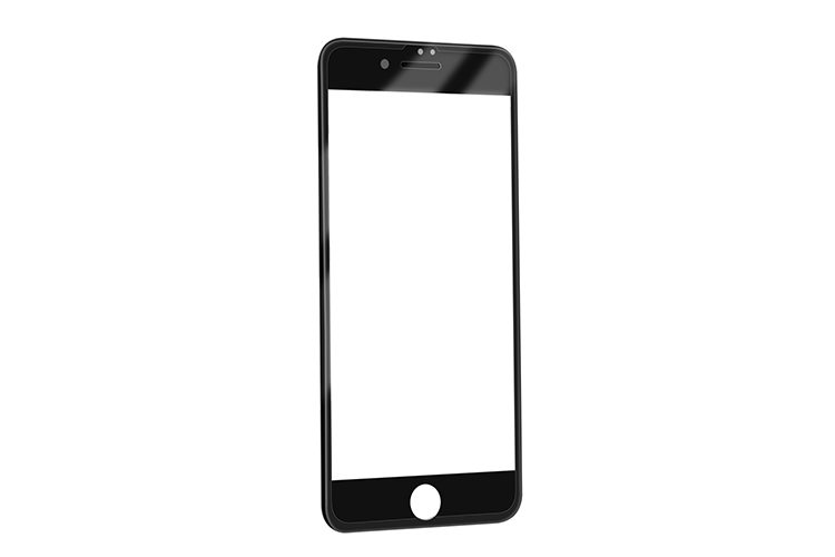
According to the needs of various terminal applications, glass cover panels require various optical glass processing processes such as cutting, edging, drilling, polishing, thinning, chemical strengthening, printing, laser engraving and coating. Today we will introduce the thinning and coating of mobile phone cover glass, which are the most important parts of the whole manufacturing process.
Cover glass thinning process
The glass mentioned in this article is not the 3mm, 5mm, 8mm or even 10mm glass for civil use, but the cover glass for electronic products such as smartphones and tablet computers. Among the glasses currently on the market, the thinnest is 0.15 mm. There is a special thinning process that reduces the thickness of the glass.
Since Steve Jobs started using Corning Gorilla Glass for his iPhones, there emerges a new component for electronic products—cover glass. At the same time, the pursuit of thinner and lighter in the industry is also urging glass manufacturers to make changes to make thinner cover glass.
iPhone cover glass
Currently, the thinnest glass of gorilla can be made 0.4mm, and the Asahi Glass can make 0.2mm glass. In general, people’s expectations for cover glass are nothing more than two:
1. Reduce the space occupied by the glass.
2. Make the glass cover a certain flexibility.
Mobile phone cover glass thinning process
There are not many processes for glass cover thinning: pre-cleaning—etching and thinning—–secondary cleaning——-grinding (single or double sided)—–post-cleaning—–check the package
Pre-cleaning: Remove the stain on the surface of the glass cover. It is one of the key steps affecting the effect of thinning.
Etching and thinning: using acid and alkali to etch the glass cover achieve the purpose of thinning. The conditions and parameters (time, potash ratio, temperature, etc.) vary from manufacturer to manufacturer, which is the technical secret of the manufacturer.
Secondary cleaning: Clean the residue of the glass cover.
Grinding: To obtain a bright, flat surface. It is one of the key processes for appearance assurance and thickness tolerance control.
Post-cleaning: Clean the remaining grinding powder.
Check the packaging: The standard for the appearance of the glass is different depending on the requirements of the customer.
Mobile phone cover glass thinning treatment
1, multiple pieces of upright soak
2, waterfall flow processing
3, single piece vertical spray
Cover glass coating process
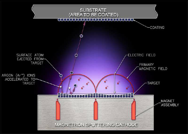
At present, vacuum magnetron sputtering coating technology is a widely used thin film deposition technology. The continuous development of sputtering technology and the exploration of new functional films have enabled the application of magnetron sputtering coating technology to be extended to many productions and scientific research fields.
magnetron-sputtering-system
magnetron sputtering coating applications
In the field of microelectronics, as a non-thermal coating technology, magnetron sputtering coating technology is mainly applied to materials that are not suitable for chemical vapor deposition or metal organic chemical vapor deposition. Moreover, using magnetron sputtering can obtain a large-area uniform film.
Magnetron sputtering technology is also used in optical films such as antireflection glass, low emissivity glass and transparent conductive glass. In the production of transparent conductive glass, the ITO conductive glass prepared by sputtering has an average transmittance of 90% or more in the visible light range.
In the modern machining industry, the use of magnetron sputtering technology to produce surface functional films, super hard films and self-lubricating films can effectively improve surface hardness, composite toughness, wear resistance and high temperature resistance and chemical stability, thus improve the service life of coated products.
In addition, magnetron sputtering coating technology also plays an important role in the research of high temperature superconducting thin films, ferroelectric thin films, giant magnetoresistive thin films, thin film luminescent materials, solar cells, and memory alloy thin films.
Magnetron sputtering coating advantages
Magnetron sputtering coating technology has become one of the main technologies of the industrial coating due to its remarkable advantages:
(1) Simple operation and easy control. In the coating process, if the sputtering conditions such as working pressure and electric power are relatively stable, the deposition rate is relatively stable.
(2) The deposition rate is high. When depositing most of the metal, especially the high melting point metal and oxide, such as tungsten, aluminum TiO2 and ZrO2 film, it has a high deposition rate.
(3) Low temperature of the substrate. Compared to two-pole sputtering or thermal evaporation, magnetron sputtering reduces the heating of the substrate, which is quite advantageous for achieving the sputter coating of the fabric.
(4) The sputtered film is strong. The sputtered film has excellent adhesion to the substrate and its mechanical strength is also improved.
(5) The sputtered film is dense and uniform. From the photomicrograph, the surface morphology of the sputtered film is fine and uniform.
(6)The sputtered films all have excellent properties. For example, sputtered metal films generally achieve good optical properties, electrical properties, and certain special properties.
(7) Easy to mass produce. The magnetron source can be expanded as required, so large-area coatings are achievable. In addition, sputtering can work continuously, and the coating process is easy to control automatically, so that the industrial assembly line can be realized.
(8) Environmentally friendly. Conventional wet plating produces waste liquid, waste residue, and exhaust gas, causing serious pollution to the environment. The magnetron sputtering coating method has high production efficiency while does not cause environmental pollution.
It’s overwhelming how many smartphone models are currently available on the market today. However, as for the color of the phone, what get are the same old black, white, silver and gray, in glossy or matte.
Well, recently an exciting new trend has emerged. The Huawei P20 series let people see the optimal color design and professional photography.A few months ago, Huawei launched the P20 in Twilight, and the dual-tone gradient inspired by the Aurora Borealis made people feel excited.
Huawei P20
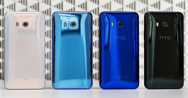
Before that, HTC also introduced the two-tone gradient scheme. Although it does not offer the popular Twilight color scheme, it does bring us a few appealing options with its latest flagship device.
HTC U11
Samsung has also jumped on board the gradient crazy. The Korean tech giant has unveiled a new version of its Galaxy A9 Star in China which features a sleek purple gradient.
Galaxy A9 Star2
Well, these are just a few examples to show that gradient color is the fashion of the year 2018. Are you curious about how to achieve this kind of gradient color? Is it difficult?
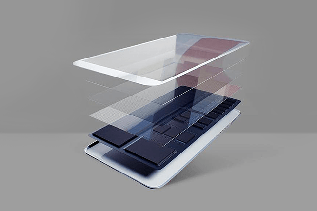
Film coating-Physical vapor deposition
Actually, all the color of the shell is about film coating. A cellphone is made from a variety of metals, with the most common being aluminum alloys, lightweight materials commonly found in the phone case. And the film coating is to apply a colored film on the phone case.
Physical vapor deposition is the most widely used film coating technology. Under vacuum conditions, the surface of the material (usually referred to as the sputtering targets or evaporating pellets) is vaporized into gaseous atoms by physical methods, and is then deposited on the surface of the substrate to form a thin film. The main methods of physical vapor deposition include vacuum evaporation, sputtering coating, plasma coating, ion plating, and molecular beam epitaxy.
How to coat the gradient color
PVD can coat gold, brass, rose gold, silver white, black, smoky, copper, brown, purple, blue, burgundy, bronze and other colors on stainless steel, copper, zinc alloy and other metals. There are many choices and the price is affordable, compared to pure gold or other pure metals. (PVD Coating Materials.pdf) You can refer to our previous article for more information:Introduction to PVD Coatings.
By controlling the parameters of different targets and thickness of the deposited film, the film exhibits different colors (the gradation colors mentioned above) under the reflection, refraction and interference of light. Specifically, in the plating furnace space, bombard a specific sputtering target with ultra-high speed electrons; use a certain mask to cover a part of the ion cloud so that only the other part of the ion cloud can be attached to the substrate and forms a very thin layer of nano-plating; control the thickness of the coating to form a nanometer thickness difference; then spray the background color.