What is PVD coating technology
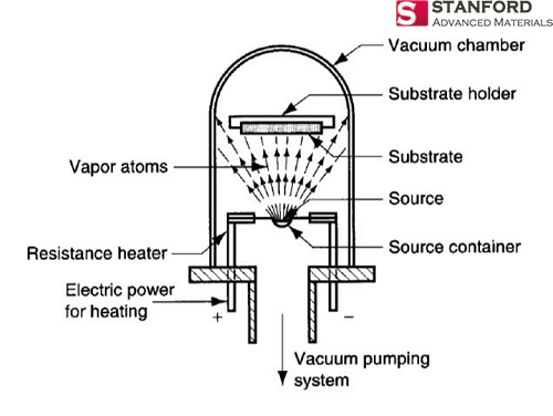
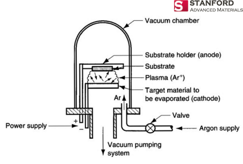
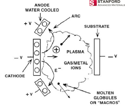
PVD, or physical vapor deposition, is an advanced surface treatment technology widely used in the world. Under a vacuum condition, utilize the gas discharge to separate the gas or the evaporated substance, then accelerate the gas ion or the evaporated atoms to bombard the substrate and deposit a film. PVD film has fast deposition speed as well as strong adhesion, good diffraction, and wide application range.
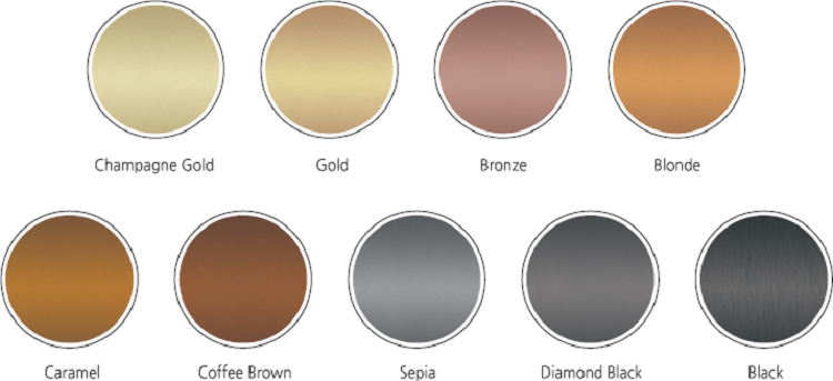
PVD coating colors
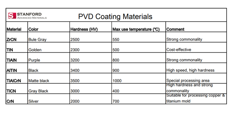
PVD can coat gold, brass, rose gold, silver white, black, smoky, copper, brown, purple, blue, burgundy, bronze and other colors on stainless steel, copper, zinc alloy and other metals. There are many choices and the price is affordable, compared to pure gold or other pure metals. (PVD Coating Materials.pdf)
Applications
PVD technology is widely used in the processing of door and window hardware, lamps, jewelry, handicrafts, and other decorative products.
PVD is now quite popular in the hardware field, and many of the world’s leading hardware manufacturers have begun to develop PVD products and mass production.
PVD for molds and precision parts
In recent years, PVD coating technology has been applied more and more in the work surface strengthening treatment of molds. Its outstanding advantages are that it can effectively improve the service life of the mold, and at the same time reduce the coating temperature to about 250 °C ~ 500 °C, which can reduce the deformation of the workpiece. The PVD composite coating has excellent performance and has potential applications that cannot be underestimated. One of the main applications of PVD technology in the mold industry is TiN coating.
PVD & CVD
There are currently two coating methods commonly used in production: physical vapor deposition (PVD) and chemical vapor deposition (CVD). The former has a deposition temperature of 500 ° C and a coating thickness of 2 to 5 μm; the latter has a deposition temperature of 900 ° C to 1100 ° C, a coating thickness of 5 to 10 μm, and the device is simple and the film is uniform.
Previously, most cemented carbides are coated by CVD. However, since the deposition temperature is high, the cemented carbide coated by the CVD method, a brittle decarburization layer (η phase) is easily formed between the coating layer and the substrate, resulting in brittle fracture of the blade. In the past decade or so, with the advancement of coating technology, the cemented carbide can also adopt the PVD method.
Development of cemented carbide coatings
Coating refers to the application of a thin layer of wear-resistant, refractory metal or non-metallic compound on the substrate of cemented carbide or high-speed steel by vacuum evaporation and sputtering.
A good coating material is required to have high hardness, good wear resistance, stable chemical properties, no chemical reaction with the workpiece material, heat and oxidation resistance, low friction factor, and strong adhesion to the substrate. However, a single coating material is difficult to meet the above requirements. Therefore, the development of cemented carbide coating materials has entered a new stage of thick film, composite film and multi-component coating.
The most mature and widely used cemented carbide coating material is TiN, but the bonding strength of TiN and the substrate is less than that of TiC. TiC coatings have high hardness and wear resistance, and good oxidation resistance, but they are brittle and not resistant to impact. Both of these kinds of coatings have advantages and disadvantages, and TiCN combines their merits.
Combine 1)the newly developed multi-component, ultra-thin TiCN, TiAlN coating, 2)TiC, TiN, Al2O3 coatings, and 3)a new anti-plastic deformation matrix can significantly improve the toughness, bond strength of the coating to the substrate, and wear resistance of the coating. At present, the technology of coating diamond film on the cemented carbide substrate is successfully realized, and the performance of the tool is comprehensively improved.
TiAlN, CrN, and TiAlCrN are also new materials for cemented carbide coatings developed in recent years. The chemical stability and oxidation resistance of TiAlN are good. Compared with TiN, the tool life can be improved by 3 to 4 times when processing high alloy steel, stainless steel, titanium alloy and nickel alloy with TiAlN.
CrN is a titanium-free coating with good chemical stability and no sticking. It is suitable for cutting titanium and titanium alloys, copper, aluminum and other soft materials.
TiAlCrN is a gradient structure coating, which not only has high toughness and hardness, but also has a small friction factor. It is suitable for milling cutters, hobs, taps and other tools, and its cutting performance is obviously better than TiN.
In addition to the above new coatings, there are some coatings with specific functions, such as MoS2, DLC lubricated coatings, which have a small friction factor (0.05) and are suitable for coating tools such as taps and drills to improve chip evacuation performance.
For more information, please visit https://www.sputtertargets.net/.


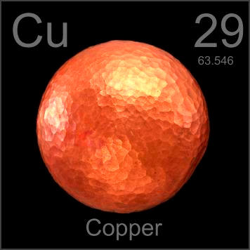 Cyprus is the original source material for the chemical element Copper. The people of Middle East initially discovered it in 9000 BC. “Cu” is the canonical chemical symbol of copper.
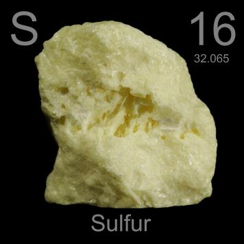 Whereas Sulfur, otherwise known as sulphur, is first introduced in 2000 BC and discovered by Chinese and Indians. It is a chemical name originated from the Sanskrit word ‘sulvere’, and the Latin ‘sulfurium’. Both names are for sulfur.