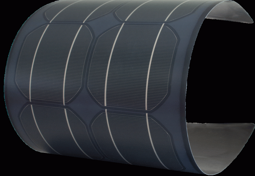
With the full arrival of the mobile energy era, the thin film solar industry grows explosively. Thin-film solar chips are light, thin, and flexible. They can be embedded in various types of carriers like Intel chips, from urban skyscrapers to neighborhood roofs, or parasols on the street, and cars running on the road. They have turned traditional products into “power generation bodies”, enabling energy sharing and free use.

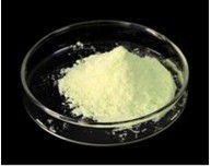
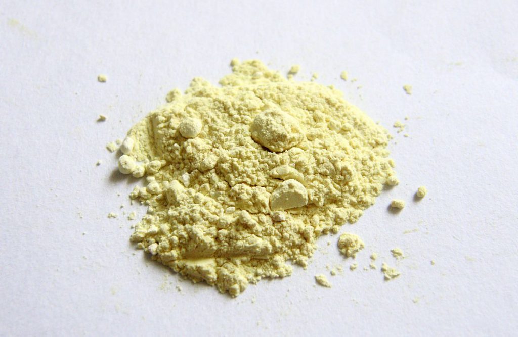
Indium is one of the basic raw materials for the manufacture of thin film solar cells. Indium, atomic number 49, was discovered in 1863 by the German chemist H. Richter in zinc concentrate. Indium is silvery white and has a light blue color. The texture is very soft and can be scored with nails. In nature, indium minerals are dispersed in trace amounts in other minerals. The distribution of indium in the earth’s crust is relatively small, 1/8 of gold and 1/50 of silver. So far, no single or indium-based natural indium deposit has been found. Therefore, indium resources, in people’s impression, are scarce and difficult to mine, so that there is concern about whether there will be shortages and unstable prices of the precious metal.
Luckily, it is optimistic that the industry has said that with the improvement of mining technology, drilling technology, purification technology and recycling technology, more and more indium resources can be used. Therefore, even if the output of copper indium gallium selenide (CIGS) increases explosively in the next few years, it is difficult to affect the supply and demand of indium.
CIGS solar cellIn the future, the copper indium gallium selenide film industry will enter a period of low-cost and high-speed development, and the thin-film solar market will be fully opened. As the photovoltaic industry continues to evolve, reducing power generation costs is a continuing goal. In this context, reducing the amount of precious indium through technical routes is a cost-reduction method that many companies are actively exploring.
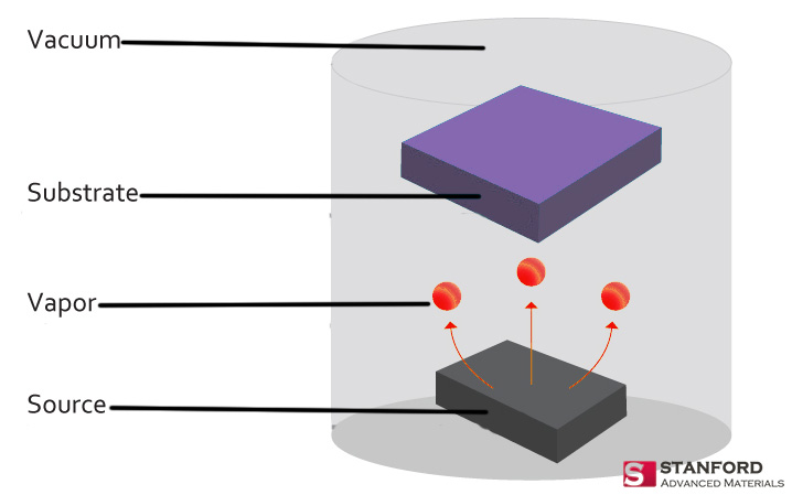
At present, some companies have developed a more reliable solution to reduce the amount of indium used in copper-indium-gallium-selenide modules: developing new plasma-spray target technology, reducing the loss in sputtering target coating, reclaiming indium on residual targets, and etc. In addition, by appropriately increasing the composition of gallium or thinning the battery film layer in the copper indium gallium selenide battery, the amount of indium can also be effectively reduced.
The industry produces metal indium by purifying waste zinc and waste tin, and the recovery rate is about 60-70%. From this calculation, based on the proven reserves, the increase in recoverable amount and the indium recovery rate, the currently available indium is about 15,000 tons to 18,000 tons. If all of these indiums are used to produce copper indium gallium selenide batteries, it can produce 1,800 GW, and even if only one-tenth of the amount is used, it can produce 180 GW. In conclusion, in terms of current copper indium gallium selenide production capacity, indium resources are still very rich.
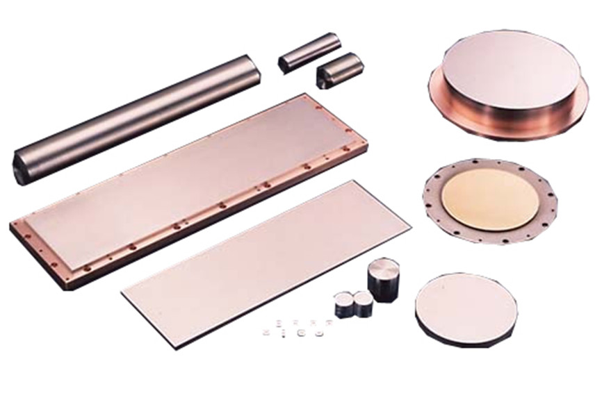
For more information about thin film coating, please visit https://www.sputtertargets.net/.