Rare earth definition
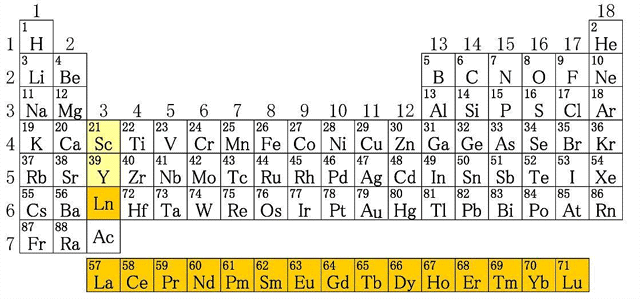
Rare earth contains 17 metal elements of lanthanides as well as scandium and yttrium. Scandium and yttrium are included in rare earth element because they are often symbiotic with lanthanide elements in mineral deposits, thus have similar chemical properties.
Discovery of Yttrium
There are 250 kinds of rare earth minerals in nature. The first to discover rare earths element was the Finnish chemist John Gadolin, who separated the rare earth element yttrium (Y) from a bituminous heavy ore (Yttria, Y2O3) in 1794.
Origin of the name
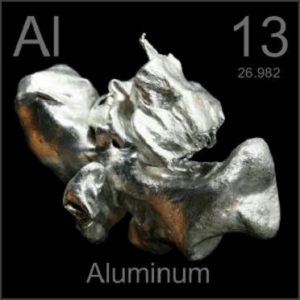
There were few rare earth minerals discovered in the 18th century, and using chemical methods can only a small amount of water-insoluble oxides could be produced. At that time, people often referred to water-insoluble solid oxides as earth. For example, aluminum was called “ceramic earth” and calcium oxide was called “alkaline earth”. At that time, rare earths are generally separated as oxides, and because of the small quantity, they were thus named Rare Earth (RE or R).
Rare earth is not rare
The content of rare earth elements in the earth’s crust is not that scarce as the name suggests. The total Clark value of rare earth is 234.51%, which is more than common elemental copper (Clarke value 10%), zinc (Clarke value 5%), tin (Clark value 4%) and cobalt (Clarke value is 3%). However, the distribution of rare earth elements is too scattered, and these seventeen elements always exist at the same time, so the total purity is not high. In general, minerals containing 10% rare earths can be called rare earth-rich ores; pure rare earth products are expensive due to their similar properties and difficulty in extraction.
Physicochemical property
- Lack of sulfides and sulfates, indicating that the rare earth elements have oxytropism;
- The silicate of rare earth is mainly island-shaped, without layered, frame-like and chain-like structures;
- Some rare earth minerals (especially complex oxides and silicates) exhibit an amorphous state;
- The rare earth minerals mainly include silicates and oxides in magmatic rocks and pegmatites, and fluorocarbonates and phosphates in hydrothermal deposits and weathering crust deposits;
- Rare earth elements are often symbiotic in the same mineral due to their similar atomic structure, chemical and crystal chemical properties. That is to say that the rare earth elements of the cerium and the yttrium are often present in one mineral. But these elements do not coexist in equal amounts– some minerals are mainly composed of cerium, and some minerals are mainly yttrium.
Please visit http://www.sputtering-targets.net/ for more information.


 Discovery

 Discovery of vanadium