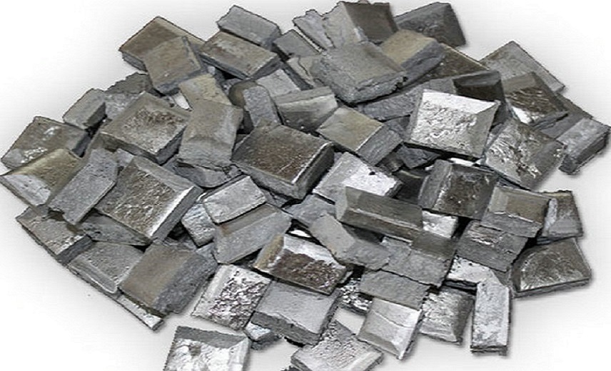
SAM®Titanium is a new type of metal. Its properties are related to the content of other impurities, such as carbon, nitrogen, hydrogen and oxygen. The purest titanium iodide has an impurity content of less than 0.1%, but it has low strength and high plasticity.
The general properties of 99.5% industrial pure titanium are as follow:
| Stanford Advanced Materials | |
| density ρ | 4.5g/cm3 |
| melting point | 1725°C |
| thermal conductivity λ | 15.24W/(mK) |
| tensile strength σb | 539MPa |
| elongation δ | 25% |
| section shrinkage ratio ψ | 25% |
| elastic modulus E | 1.078×10⁵ MPa |
| hardness HB | 195 |
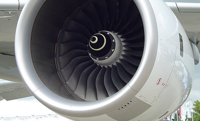
(1) High specific strength
The density of titanium alloy is generally about 4.5g/cm3 (only 60% of steel), but the strength of pure titanium is close to that of normal steel. And some high-strength titanium alloys have higher strength than many alloy structural steels. Therefore, the specific strength (strength/density) of titanium alloy is much larger than that of other metal structural materials. It can be used to produce parts and components with high unit strength, good rigidity and lightweight. At present, titanium alloys are used for aircraft engine components, skeletons, skins, fasteners and landing gear.
(2) High-temperature strength
Titanium alloys can be used in higher temperature environments than aluminum alloys. Titanium alloys can retain the required strength and maintain long-term operation at the temperatures between 450 and 500 °C. While the specific strength of the aluminum alloy is significantly reduced when the temperature reaches 150 ° C.
(3) Good corrosion resistance
Titanium alloy can work in the moist atmosphere and seawater medium with good corrosion resistance, which is much better than stainless steel. It is especially resistant to pitting, acid etching and stress corrosion. In addition, titanium also has excellent corrosion resistance to alkali, chloride, chlorine organic substances, nitric acid, sulfuric acid, and the like. The fly in the ointment is that titanium has poor corrosion resistance to reducing oxygen and chromium salt media. For more information about the corrosion resistance of titanium, please read this passage Does titanium never corrode?
(4) Good low-temperature performance
Titanium alloys retain their mechanical properties at low and ultra-low temperatures. Titanium alloys with good low-temperature properties and extremely low interstitial elements. For instance, TA7 can retain a certain degree of plasticity at -253 °C. Therefore, the titanium alloy is also an important low-temperature structural material.
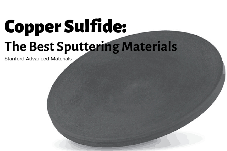
Please visit https://www.sputtertargets.net/ for more information.
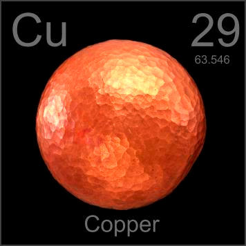 Cyprus is the original source material for the chemical element Copper. The people of Middle East initially discovered it in 9000 BC. “Cu” is the canonical chemical symbol of copper.
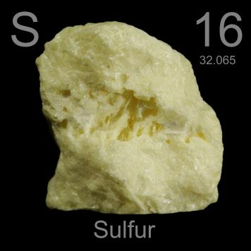 Whereas Sulfur, otherwise known as sulphur, is first introduced in 2000 BC and discovered by Chinese and Indians. It is a chemical name originated from the Sanskrit word ‘sulvere’, and the Latin ‘sulfurium’. Both names are for sulfur.