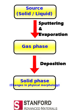
Physical vapor deposition processes use vacuum technology to create a sub-atmospheric pressure environment and an atomic or molecular condensable vapor source (from a solid or liquid surface) to deposit thin films and coatings. Sputtering deposition and vacuum evaporation are among the more well known.
Sputtering deposition
The sputtering deposition is an etching process that alters the physical properties of a surface. In this process, a gas plasma discharge is set up between two electrodes: a cathode plating material (the sputter coater targets) and an anode material (the substrate). The film made by sputter coating are thin, ranging from 0.00005 – 0.01 mm. Chromium, titanium, aluminum, copper, molybdenum, tungsten, gold, and silver are typical sputter coating targets.
Sputter coated films are used routinely in decorative applications such as watchbands, eyeglasses, and jewelry. Also, the electronics industry relies on heavily sputtered coatings and films, such as thin film wiring on chips and recording heads as well as magnetic and magneto-optic recording media. Companies also use sputter deposition to produce reflective films for large pieces of architectural glass used in the automotive industry. Compared to other deposition processes, sputter deposition is relatively inexpensive.
Vacuum Evaporation
The vacuum evaporation is a process of reducing the wastewater volume through a method that consists of concentrating a solution by eliminating the solvent by boiling. In this case, it is performed at a pressure lower than atmospheric pressure. Thus, the boiling temperature is much lower than that at atmospheric pressure, thereby resulting in notable energy savings. The basic components of this process consist of: evaporation pellets, heat-exchanger, vacuum, vapor separator, and condenser.
Vacuum evaporation is used in the semiconductor, microelectronics, and optical industries and in this context is a process of depositing thin films of material onto surfaces. High-purity films can be obtained from a source evaporation material with high purity. The source of the material that is going to be vaporized onto the substrate can be a solid in any shape or form (usually pellets). The versatility of this method trumps other deposition processes. Also, when the deposition is not desired, masks are utilized to define the areas on the substrate for control purposes.
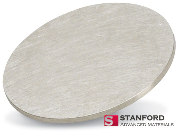
Siver is a very malleable metallic chemical element with atomic number 47 that is capable of a high degree of polish, has the highest thermal and electric conductivity of any substance. Silver sputtering target is used as decorative coatings and antibiotic coating in medical devices.
Physical vapor deposition (PVD) of thin films, laser ablation deposition (PLD), magnetron sputtering for semiconductor, display, LED and photovoltaic devices.
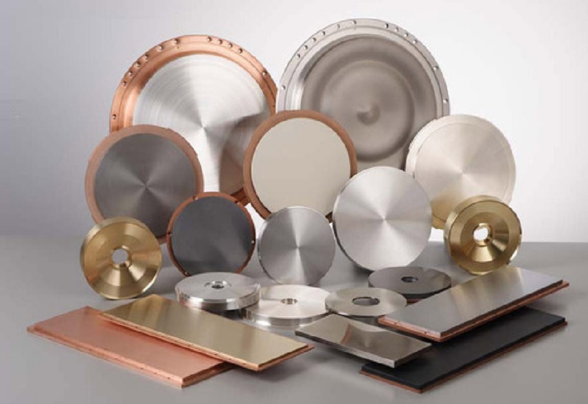
Each target can be designed to fit customer specified backing plates or cups with either indium/tin or silver epoxy bonding. Bonding service is available on oxygen free copper backing plate.
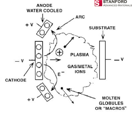
Pulsed laser deposition (PLD) is a physical vapor deposition (PVD) technique where a high-power pulsed laser beam is focused inside a vacuum chamber to strike a target of the material that is to be deposited. Although the equipment of pulsed laser deposition (PLD) system is simple, its working mechanism is related to many complicated physical phenomena. It includes all physical interactions between the laser and the substance when the high-energy pulsed radiation strikes the solid sputtering target, the formation of plasma plumes and the transfer of the molten material through the plasma plume to the surface of the heated substrate. Therefore, PLD can generally be divided into the following three stages:
Interaction between laser radiation and the sputtering target
In this stage, the laser beam is focused on the surface of the target materials. When sufficient high energy flux and short pulse width are achieved, all elements of the target surface are rapidly heated to the evaporation temperature. At this point, the material in the target will be sputtered from the target. The instantaneous melting rate of the target is highly dependent on the flow of laser light onto the target. The melting mechanism involves many complex physical phenomena such as collisions, heat, excitation with electrons, delamination, and fluid mechanics.
Dynamics of molten matter
In the second stage, according to the law of aerodynamics, the sputtered particles have a tendency to move toward the substrate. The space thickness varies with the function cosn θ, and n>>1. The area of the laser spot and the temperature of the plasma have an important influence on the uniformity of the deposited film. The distance between the target and the substrate is another factor that affects the angular extent of the molten material. It has also been found that placing a baffle close to the substrate narrows the angular extent.
Deposition of molten material on the substrate
The third stage is the key to determining the quality of the film. The high-energy nuclides emitted hit the surface of the substrate and may cause various damages to the substrate. The high energy nuclide sputters some of the atoms on the surface, and a collision zone is established between the incident stream and the sputtered atoms. The film is formed immediately after the formation of this thermal energy zone (collision zone), which is the best place to condense particles. As long as the condensation rate is higher than the release rate of the sputtered particles, the heat balance condition can be quickly reached, and the film can be formed on the surface of the substrate due to the weakened flow of the molten particles.
Although the rotary targets have developed in recent years, the mainstream shape of the sputtering target is still the planar type. Today let us take a look at the pros and cons of planar targets to help you determine whether a planar sputtering target is suitable for your project.
Advantages of Planar Sputter Target
Simple structure – one of the main advantages of the planar target is that the structure is simple. The common planar targets on the market are rectangular planar targets and circular planar targets, which are easily produced by molds. In other words, planar target preparation requires fewer machines and technologies and is easier to prepare. This is why planar targets still dominate the sputtering target market.
Molds
Low price – You can never deny that the price is always an important competitive factor. As mentioned above, the manufacturing process of the planar sputter target is easier, so its price is much lower than the rotatory sputter target.
Strong versatility – Planar sputtering targets usually have strong versatility. Therefore, the transportation of the planar targets is relatively simple and is not easily damaged during transportation.
Good uniformity and repeatability – Film layers sputtered by planar targets usually boast good uniformity and repeatability. Planar targets are still best suited for prototype work or elemental experimentation, especially when large amounts of material are not needed at once.
Disadvantages of Planar Sputter Target
Its biggest disadvantage is the low utilization rate (generally only about 20%). In the sputtering process of the planar target, a strip-shaped pit will be formed when the target of the glow region (the magnetic field distribution region) is consumed to a certain extent, making the target body thinner. And once the pit depth reaches a certain value, the target cannot be utilized anymore. The low utilization rate also reduces its price advantage to some extent.
In conclusion, planar targets are still the best choice for prototype work or elemental experimentation, especially when large amounts of material are not needed at once. But its disadvantage of low utilization rate (20% vs. 80% compared with the rotatory target) does constrain its development.
Next week, let us look at the biggest competitor of the planar target– the rotatory target. Weighting the pros and cons of these two types of sputtering target may help you better choose the one for your application.
NiCrSi high-resistance sputtering targets are mainly used to prepare metal film resistors and metal oxide film high resistance resistors, integrated circuit wiring and sensors. These devices are very important in electronic computers, communication instruments, and electronic switches. Due to its excellent performance, resistors made from NiCrSi high-resistance sputtering targets have gradually become a new generation of universal resistors that replace carbon film resistors. Here are two methods for preparing NiCrSi high-resistance sputtering targets.
Adding rare earth metals to improve the target performance
Raw materials: chromium and nickel with an elemental purity greater than 99.5%; silicon with an elemental purity greater than 99.9%; rare earth metals with a mixture purity greater than 98%.
Step 1: Smelt Ni, Cr and a small amount of Si into an intermediate NiCrSi alloy. The voltage during the melting of the electric arc furnace is 20V, the current is 500~600A, and the time is 2~5min.
Step 2: Place the prepared intermediate NiCrSi alloy was in the bottom of the feeder in a vacuum induction melting furnace. Add the refractory Si material after the intermediate alloy is melted. The vacuum degree during vacuum induction melting is 2 × 10 -2 torr, the power is 35 kW, and the time is 1 h.
Step 3: Refining. The power is 20 kW and the time is 30 min.
Step 4: Add the rare earth metal in the refining stage. Stir the solution is uniformly by electromagnetic induction and inject it into the investment mold. After the mold is cooled, release the mold to obtain the casting mold.
Step 5: Heat treat and machine the target casting. The heat treatment process has a temperature of 800 ° C and a time of 2 h.
Step 1: Use a corundum-graphite-magnesia composite intermediate frequency vacuum induction furnace. Place the prepared materials in a corundum crucible and smelt them under a vacuum of 1×10⁻² torr. The melting temperature is 1,500 to 1,550 ° C, the time 1 h, the power of the medium frequency induction furnace is 10~40kW, and the voltage and current of the induction coil are 100~400V and 200~380A respectively.
Step 2: Set a casting tube in the mold shell and extend the nozzle to the bottom surface of the mold shell. Then bake the mold shell to reach 650-700 ° C for casting. After that, cool the mold shell slowly to 850-800 ° C and kept the temperature for 1 h. Then cool it to the room temperature.
Target Bonding for NiCrSi Target
To increase the strength of the target, the NiCrSi target requires a copper plate to be soldered on the back side. The shape and size of the copper plate are the same as the target, and the thickness is 1~3mm. The target and the copper plate are welded firmly by indium bonding or elastomeric bonding, and the soldering temperature is 250 to 270 ° C for 4 hours.
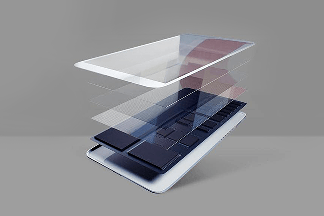
According to the needs of various terminal applications, glass cover panels require various optical glass processing processes such as cutting, edging, drilling, polishing, thinning, chemical strengthening, printing, laser engraving and coating. Today we will introduce the thinning and coating of mobile phone cover glass, which are the most important parts of the whole manufacturing process.
Cover glass thinning process
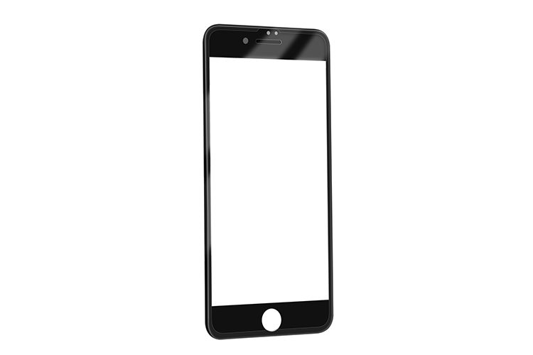
The glass mentioned in this article is not the 3mm, 5mm, 8mm or even 10mm glass for civil use, but the cover glass for electronic products such as smartphones and tablet computers. Among the glasses currently on the market, the thinnest is 0.15 mm. There is a special thinning process that reduces the thickness of the glass.
Since Steve Jobs started using Corning Gorilla Glass for his iPhones, there emerges a new component for electronic products—cover glass. At the same time, the pursuit of thinner and lighter in the industry is also urging glass manufacturers to make changes to make thinner cover glass.
iPhone cover glass
Currently, the thinnest glass of gorilla can be made 0.4mm, and the Asahi Glass can make 0.2mm glass. In general, people’s expectations for cover glass are nothing more than two:
1. Reduce the space occupied by the glass.
2. Make the glass cover a certain flexibility.
Mobile phone cover glass thinning process
There are not many processes for glass cover thinning: pre-cleaning—etching and thinning—–secondary cleaning——-grinding (single or double sided)—–post-cleaning—–check the package
Pre-cleaning: Remove the stain on the surface of the glass cover. It is one of the key steps affecting the effect of thinning.
Etching and thinning: using acid and alkali to etch the glass cover achieve the purpose of thinning. The conditions and parameters (time, potash ratio, temperature, etc.) vary from manufacturer to manufacturer, which is the technical secret of the manufacturer.
Secondary cleaning: Clean the residue of the glass cover.
Grinding: To obtain a bright, flat surface. It is one of the key processes for appearance assurance and thickness tolerance control.
Post-cleaning: Clean the remaining grinding powder.
Check the packaging: The standard for the appearance of the glass is different depending on the requirements of the customer.
Mobile phone cover glass thinning treatment
1, multiple pieces of upright soak
2, waterfall flow processing
3, single piece vertical spray
Cover glass coating process
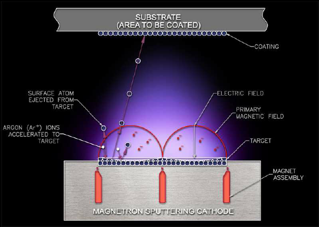
At present, vacuum magnetron sputtering coating technology is a widely used thin film deposition technology. The continuous development of sputtering technology and the exploration of new functional films have enabled the application of magnetron sputtering coating technology to be extended to many productions and scientific research fields.
magnetron-sputtering-system
magnetron sputtering coating applications
In the field of microelectronics, as a non-thermal coating technology, magnetron sputtering coating technology is mainly applied to materials that are not suitable for chemical vapor deposition or metal organic chemical vapor deposition. Moreover, using magnetron sputtering can obtain a large-area uniform film.
Magnetron sputtering technology is also used in optical films such as antireflection glass, low emissivity glass and transparent conductive glass. In the production of transparent conductive glass, the ITO conductive glass prepared by sputtering has an average transmittance of 90% or more in the visible light range.
In the modern machining industry, the use of magnetron sputtering technology to produce surface functional films, super hard films and self-lubricating films can effectively improve surface hardness, composite toughness, wear resistance and high temperature resistance and chemical stability, thus improve the service life of coated products.
In addition, magnetron sputtering coating technology also plays an important role in the research of high temperature superconducting thin films, ferroelectric thin films, giant magnetoresistive thin films, thin film luminescent materials, solar cells, and memory alloy thin films.
Magnetron sputtering coating advantages
Magnetron sputtering coating technology has become one of the main technologies of the industrial coating due to its remarkable advantages:
(1) Simple operation and easy control. In the coating process, if the sputtering conditions such as working pressure and electric power are relatively stable, the deposition rate is relatively stable.
(2) The deposition rate is high. When depositing most of the metal, especially the high melting point metal and oxide, such as tungsten, aluminum TiO2 and ZrO2 film, it has a high deposition rate.
(3) Low temperature of the substrate. Compared to two-pole sputtering or thermal evaporation, magnetron sputtering reduces the heating of the substrate, which is quite advantageous for achieving the sputter coating of the fabric.
(4) The sputtered film is strong. The sputtered film has excellent adhesion to the substrate and its mechanical strength is also improved.
(5) The sputtered film is dense and uniform. From the photomicrograph, the surface morphology of the sputtered film is fine and uniform.
(6)The sputtered films all have excellent properties. For example, sputtered metal films generally achieve good optical properties, electrical properties, and certain special properties.
(7) Easy to mass produce. The magnetron source can be expanded as required, so large-area coatings are achievable. In addition, sputtering can work continuously, and the coating process is easy to control automatically, so that the industrial assembly line can be realized.
(8) Environmentally friendly. Conventional wet plating produces waste liquid, waste residue, and exhaust gas, causing serious pollution to the environment. The magnetron sputtering coating method has high production efficiency while does not cause environmental pollution.
Happy New Year in 2019! We are very happy with your company and encouragement that push us to insist on updating every week. On the occasion of the arrival of 2019, let us summarize the Top Posts in 2018 for you.
Metal History
“Metal History” is a popular column we have opened this year, aiming at introducing the discovery of different kinds of metals. Among them, the Top 3 posts in this column are as follows:
Titanium is a metal element that is known as “space metal” because of its light weight, high strength and good corrosion resistance. The most common compound of titanium is titanium dioxide, and other compounds include titanium tetrachloride and titanium trichloride. Click the title of the article to know more.
The history of tungsten dates back to the 17th century. At that time, miners in the Erzgebirge Mountains of Saxony, Germany, noticed that some of the ore would interfere with the reduction of cassiterite and produce slag. The miners gave the mines some German nicknames: “wolfert” and “wolfrahm”. Click the title of the article to know more.
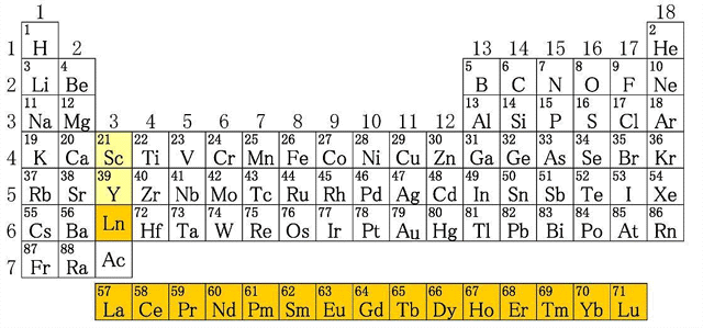
Cerium is the most abundant rare earth elements. It is a silvery gray active metal, whose powder is easily oxidized in the air and soluble in acid. Cerium has been widely used in the automotive industry as a catalyst to reduce emission, and in glass industry as glass polishing materials. Cerium sputtering target is an important material in optical coating. Click the title of the article to know more. Click the title of the article to know more.
Metal Materials Application
Apart from history, we also introduce the multiple applications of these metal materials. Among them, the Top 3 posts in this column are as follows:
At present, molybdenum target mammography is considered the recommended breast screening examinations for women’s breast cancer, one of the major causes of deaths among women, affects about 12% of women around the world. Click the title of the article to know more.
Titanium is an ideal medical metal material and can be used as an implant for the human body. Titanium alloy has been widely used in the medical field and has become the material of choice for medical products. Click the title of the article to know more.
Semiconductors have high requirements for the quality and purity of the sputtering materials, which explains why the price of anelva targets is relatively high. Click the title of the article to know more.
Sputtering Targets
Sputtering Target is the consistent keyword of our website, and thus we have shared many useful information about some specific type of sputtering targets. Our intention is to help you better understand these materials—their properties, applications, developing prospect and so on. And the followings are the posts you really have to read. Among them, the Top 3 posts in this column are as follows:
In recent years, physical vapor deposition (PVD) and chemical vapor deposition (PVD) have wide applications in various industries to increase the hardness of tools and molds or apply beautiful colors to the products. Thus these two methods are considered as the most attractive surface coating technologies. Click the title of the article to know more.
The term “indium bonding” in thin film coating industry, simply speaking, refers to bond two (or more) sputtering targets with indium (In), or one (or more) with indium plate together. Click the title of the article to know more.
At some stage in the sputtering deposition, positive ions are continuously amassed on the surface of the sputtering target. Due to the fact that those fantastic ions aren’t neutralized, the negative bias of the target surface gradually decreases, and progressively the normal operation can not be completed. This is the target poisoning phenomenon. Click the title of the article to know more.
Glad you are part of SAM’s 2018. Next year, please continue following us and we promise to give you more valuable information! Also, you can visit our official website https://www.sputtertargets.net/ for more information.
Thin film deposition technology refers to the preparation of thin films on the surface of materials used in the fields of machinery, electronics, semiconductors, optics, aviation, transportation and etc., in order to impart certain properties (such as heat resistance, wear resistance, corrosion resistance, decoration, etc.) to these materials.
The two most common forms of thin film deposition techniques are physical vapor deposition (PVD) and chemical vapor deposition (PVD).
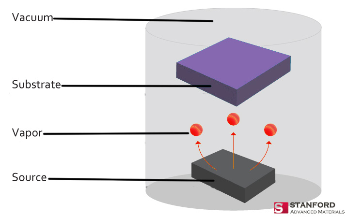
Physical Vapor Deposition —PVD
PVD is a process that achieves the transformation of the atoms from the source materials to the substrate to deposit a film by physical mechanisms such as thermal evaporation or sputtering.
PVD includes evaporation, sputtering and ion plating.
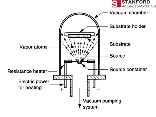
Evaporation
Evaporation is a common method of thin-film deposition. It is also called vacuum evaporation because the source material is evaporated in a vacuum. The vacuum allows the vapored particles to travel directly to the substrate, where they condense and deposit to form a thin film.
Evaporation (PVD)
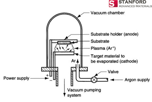
Sputtering
Sputtering is a physical vapor deposition (PVD) method of thin film deposition. It is a process whereby particles are ejected from a solid target material (sputtering target) due to the bombardment of the target by energetic particles.
Sputtering (PVD)
Ion Plating
Ion plating is a physical vapor deposition (PVD) process which uses a concurrent or periodic bombardment of the substrate, and deposits film by atomic-sized energetic particles.
Ion Plating (PVD)
Characteristics of the main physical vapor deposition method
Among the above three methods, although Ion plating’s film adhesion and density are better, due to technical limitations, the other two methods (evaporation and sputtering) are currently more widely used. In general, sputtering is the best PVD technology.
Stanford Advanced Materials (SAM) is one of the most specialized sputtering targets manufacturers, please visit https://www.sputtertargets.net/ for more information.
Sputtering is a thin film deposition process in the modern technology world of CDs, semiconductors, disk drives and optical devices industries. Sputtering is the process at an atomic level, where the atoms are automatically sputtered out from the sputtering materials and then be deposited on another substrate, such as a solar panel, semiconductor wafer or optical device. It is an effect of the severe bombard of the high energy particles on the target.
In general, sputtering occurs only when kinetic energy is said to be bombarding particles at very high speeds, which is much higher than a normal thermal energy. At the atomic level, this makes thin film deposition more precise and accurate than that by melting the source material using conventional thermal energy.
Copper Sulfide is the best material for Sputtering Targets. It can be molded into the shape of Plates, Discs, Step Targets, Column Targets and Custom-made. Copper Sulfide is a combination of two materials—Copper and Sulphur. The chemical name of the product is CuS, which offers you the Copper Sulfide product with more than 99 percent purity.
Cyprus is the original source material for the chemical element Copper. The people of Middle East initially discovered it in 9000 BC. “Cu” is the canonical chemical symbol of copper.
Whereas Sulfur, otherwise known as sulphur, is first introduced in 2000 BC and discovered by Chinese and Indians. It is a chemical name originated from the Sanskrit word ‘sulvere’, and the Latin ‘sulfurium’. Both names are for sulfur.
Copper Sulfide metal discs and plates are highly adhesive and resistant against oxidation and corrosion. Using Copper Sulfide sputtering targets to deposit thin films will not produce highly reflective and extremely conductive films, but can also extensively increase the efficiency of the source energy.
So to achieve the desired noticeable result in a sputtering deposition, the built-up process used to fabricate the Sputtering Targets should be critical. A Copper Sulfide targeted material will give the best result. However, material like only an element, alloys, mixture of elements, or perhaps a compound can be used for the purposes.
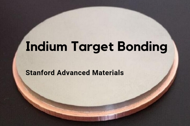
The term “indium bonding” in the thin film coating industry, simply speaking, refers to bonding two (or more) sputtering targets with indium (In), or one (or more) indium plates together.
Indium
Indium can be uniquely used in lower temperature solders, is one of the softest materials. Indium is preferred for target bonding because of its excellent thermal conductivity of all available bonds. In addition, indium is the most efficient material at drawing heat away from the sputtering target. Most materials can be indium bonded and there are just a few exceptions.
Apart from indium bonding, indium is also popular for a variety of uses and purposes, such as creating alloys, photoconductors, and thermistors.
Indium bond
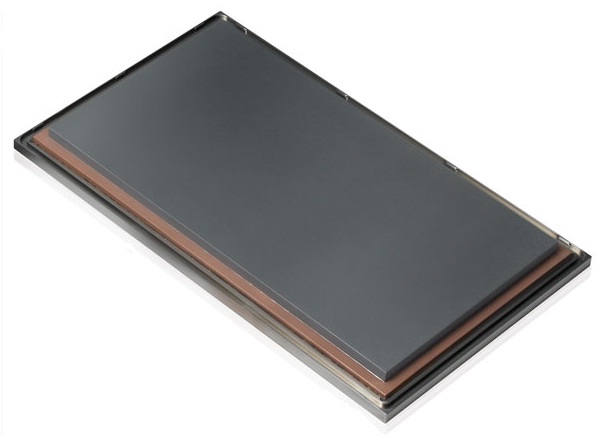
Sputtering targets can be cracked, warped, or damaged due to inadequate cooling, low hardness, or other reasons. From this point of view, although target bonding does generate a fee, it can well protect your target from damage. It is especially true for those less-strong target materials and precious metal materials.
Elastomer is an alternative bonding method that touts a higher temperature capability over the indium bond. Elastomer bonds are recommended when you are consistently melting indium bonds. We also recommend elastomer bonding for low melting point target materials, as well as, temperature-sensitive compounds and targets that have either low density or are especially fragile.
Indium bonding is preferred in applications where:
Cryogenic stability is needed
Sealing requires high levels of hermeticity
Maximum thermal transfer is required
Bonding to not-metallic surfaces
Flux cannot be used
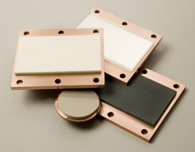
Backing plates
OFHC Copper Backing Plate is another well-known backing plate. It is frequently used to bond ceramic targets because of its non-magnetism and low coefficient of thermal expansion. This metal has good electrical and thermal characteristics while also being easy to machine, easy to soften, and readily available at a low cost. Copper backing plates can be re-used, with care, 20 or more times.
A molybdenum plate is usually used to substitute copper plate if copper is not appropriate for the application. For instance, the coefficient of expansion for copper is mismatched with some ceramics. And for high-temperature bonding, copper may also oxidize badly or warp. In these conditions, molybdenum is a more suitable material.
SAM Sputter Target
If you are looking for an indium bonding manufacturer, SAM is undoubtedly your best choice. Stanford Advanced Materials is devoted to machining standard backing plates and working together with the Taiwan Bonding Company for providing bonding services. For questions about target bonding materials, methods, and services, please see our listing of frequently asked questions (FAQs).


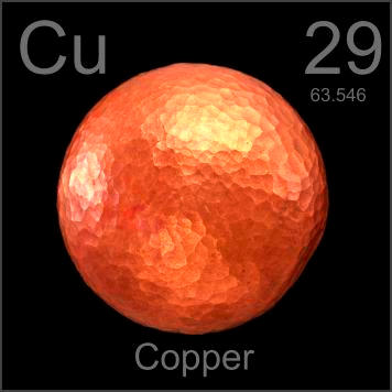 Cyprus is the original source material for the chemical element Copper. The people of Middle East initially discovered it in 9000 BC. “Cu” is the canonical chemical symbol of copper.
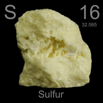 Whereas Sulfur, otherwise known as sulphur, is first introduced in 2000 BC and discovered by Chinese and Indians. It is a chemical name originated from the Sanskrit word ‘sulvere’, and the Latin ‘sulfurium’. Both names are for sulfur.