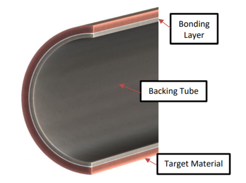
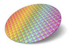
As a raw material for the deposition of hard coatings by PVD technology, the target will directly affect the physical and mechanical properties of the hard coating films. Therefore, the selection of good sputtering targets for coating preparation is of great practical significance.
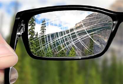
Spectacle lenses made of inorganic materials or organic materials can cause scratches on the surface of the lens due to friction with dust or gravel (silicon oxide) during daily use. Compared with glass sheets, organic materials have lower hardness and are more likely to cause scratches. Through the microscope, we can observe that the scratches on the surface of the lens are mainly divided into two types: one is because the scratches generated by the gravel are shallow and small, and the wearer is not easy to detect; the other is the scratch caused by the larger gravel, which is deep and peripherally rough, and will affect people’s vision if it is in the central area. In order to improve the anti-wear of optical lenses, people began to study optical coatings to produce anti-wear films.
Technical Development
First generation anti-wear film technology
Anti-wear films began in the early 1970s when it was thought that glass lenses were not easy to wear because of their high hardness, while organic lenses were easy to wear because they are too soft. Therefore, the quartz material is plated on the surface of the organic lens under vacuum to form a very hard anti-wear film. However, due to the mismatch between the thermal expansion coefficient and the substrate-based material, the film is easy to take off and the film layer is brittle, thus the anti-wear effect is not ideal.
Second generation anti-wear film technology
After the 1980s, researchers theoretically found that the mechanism of wear is not only related to hardness, but also related to the dual characteristics of “hardness/deformation” of the film material, that is, some materials have higher hardness but less deformation, while some materials have lower hardness but greater deformation. The second generation of anti-wear film technology is to apply a high hardness and less brittle material to the surface of the organic lens by the immersion process.
Third generation anti-wear film technology
The third generation of anti-wear film technology was developed after the 1990s, mainly to solve the problem of wear resistance after the organic lens is coated with anti-reflection film. Since the hardness of the organic lens substrate and the hardness of the anti-reflection film layer are very different, the new theory suggests that an anti-wear film layer is required between the two layers, so that the lens are not easy to be scratched. The hardness of the third-generation anti-wear film material is between the hardness of the anti-reflection film and the lens base, and the friction coefficient is low and is not easily cracked.
Hard coating film preparation technology
Physical vapor deposition is the mainstream technology of hard coating materials preparation. The main methods are sputtering, such as magnetron sputtering; and cathode arc evaporation, such as multi-arc ion plating.
Sputter Coating
Sputtering uses ions generated by an ion source (generally Ar ions), and accelerates them into a high-speed. The high-energy ion beam in a vacuum electric field bombards the surface of the sputtering target, and kinetic energy exchange between ions and target atoms. When the ion energy is sufficient, atoms on the surface of the sputtering target will leave the target and deposit on the surface of the substrate to form a thin film.
Cathodic arc evaporation
Cathodic arc evaporation is a PVD deposition method that uses arc evaporation electrode material as a deposition source. The low-voltage, high-current electron beam forms an arc on the surface of the material. When the arc moves on the surface of the target, the high current forms a local high temperature, which causes the surface of the metal ion evaporation material on the target surface to form a plasma. After that, a high-speed high-energy ion current is obtained by the electric field, and a film of the coating material is deposited on the surface of the substrate.
As a raw material for the deposition of hard coatings by PVD technology, the target will directly affect the physical and mechanical properties of the hard coating films. Therefore, the selection of good sputtering targets for coating preparation is of great practical significance.
Please visit https://www.sputtertargets.net/ for more information.