Sputtering is a high-speed process where superfast ions hit a sputtering target and dislodge minuscule particles that in turn coat a thin film on substrates like architectural glass, LED televisions and computer displays.
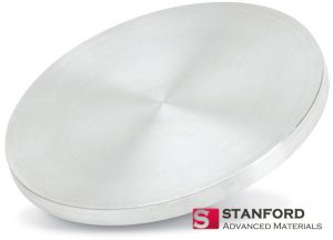
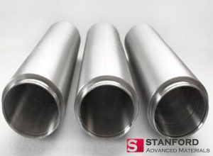
Rotatable sputtering target, or rotatory target, is a commonly used target shape in magnetron sputtering. It is generally cylindrical, with a stationary magnet inside, and a slow magnetic field, which allows the sputtering rate to be uniform and the target utilization rate to be high. Rotating targets are commonly used for coating solar cells, architectural glass, automotive glass, semiconductors, and flat-panel TVs.
The main advantage of the rotatable target is the high utilization of the target, which means that the rotating target can solve the problem of low utilization of the planar target.
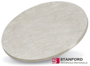
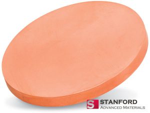
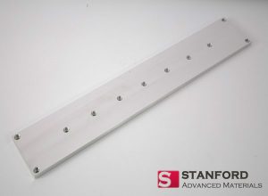
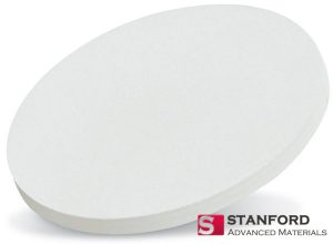
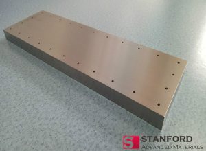
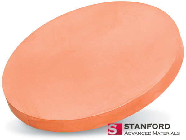
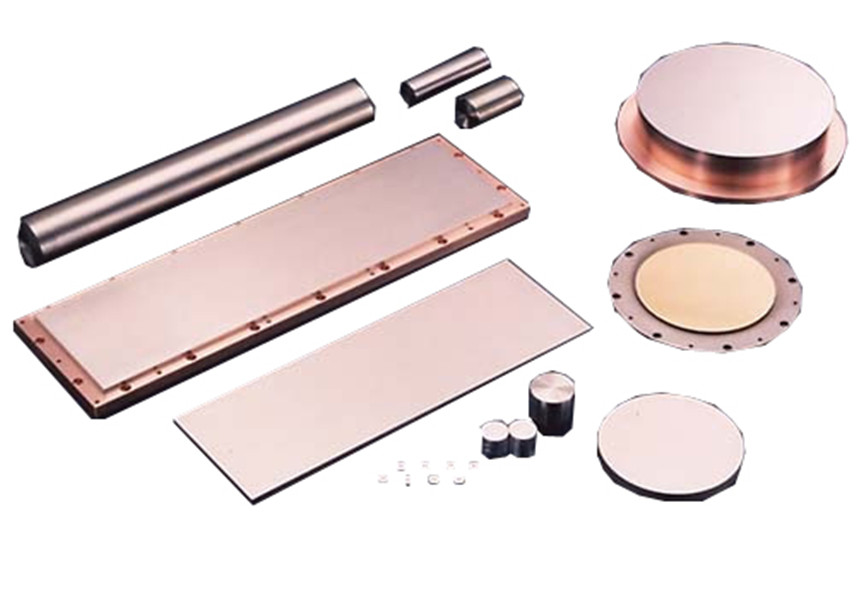
Rotatory Copper (Cu) Sputtering Target
For a planar sputtering target, the target utilization of the normal cathode can reach 25%, and the special design of the magnet bypass with the target back can increase the target utilization to about 40%. Despite this, the utilization of planar targets is still not high. However, the utilization of cylindrical rotating targets is typically in the range of 75% to 90%, much higher than planar targets. However, when the rotating target is used for large-area coating, the uniformity of the surface of the film layer is poor and it is difficult to meet the requirements, which is the biggest disadvantage of the rotating target.
The sputtering target is a key required material for vacuum film coating. It refers to a material that can ionize the surface by the current-binding magnetic field.
Almost all sputter coating equipment uses a powerful magnet to spiral the electrons to accelerate the ionization of the argon around the target, resulting in an increased likelihood of collision between the target and the argon ions, thereby increasing the sputtering rate.
Typically, most metal plating uses DC sputtering, while non-conductive ceramic materials use RF sputtering. The basic principle is that argon (Ar) ions are struck against the target surface by glow discharge in a vacuum, and cations in the plasma are accelerated as a sputter material to the surface of the negative electrode. The impact will cause the material of the target to fly out and deposit on the substrate to form a film.
Generally, the sputter coating process has several features:
(1)Many materials can be deposited into thin film materials by sputtering, including metals, alloys, insulators, and the like.
(2)Under appropriate conditions, different component target materials can be made into films of the same material.
(3)Oxides or other compounds of the target substance and gas molecules can be prepared by adding oxygen or other reactive gas to the discharge atmosphere.
(4)Highly accurate film can be obtained by controlling the magnitude of the input current and the length of the sputtering time.
(5)For large-area coatings, sputter deposition is definitely superior to other coating processes.
(6)In the vacuum vessel, the sputtered particles are not affected by gravity, and the positions of the target and the substrate can be freely aligned.
(7)The bond strength between the sputter-coated substrate and the film is 10 times or more the adhesive strength of a general evaporated deposited film. Furthermore, since the sputtered particles have high energy, the surface of the film is continuously diffused to obtain a hard and dense film. At the same time, high energy allows the substrate to obtain a crystalline film at a lower temperature.
(8)The nucleation density at the initial stage of film formation is high, and an extremely thin continuous film of 10 nm or less can be produced.
(9)Sputtering targets have a long service life and can be continuously produced over a long period of time.
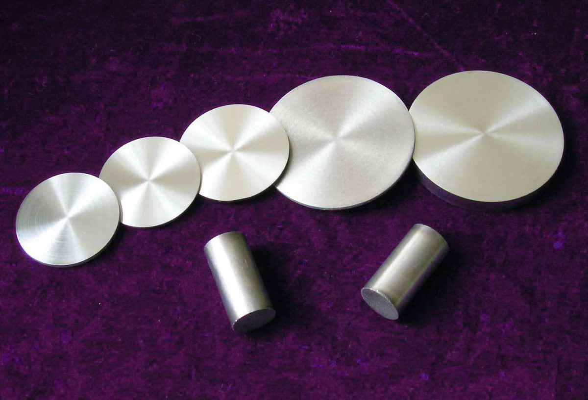
(10)The sputtering target can be made into various shapes. By special design of the shape of the target, the sputtering process can be better controlled and the sputtering efficiency can be most effectively improved.
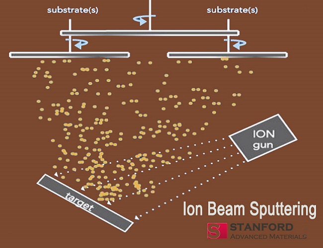
1 Ion beam sputtering relies on momentum exchange to make atoms and molecules of solid materials enter the gas phase. The average energy generated by sputtering is 10 eV, which is about 100 times higher than that of vacuum evaporation. After deposited on the surface of the substrate, these particles still have enough kinetic energy to migrate on the surface of the substrate, so that the film has good quality and is firmly bonded to the substrate.
2 Any material can be coated by ion beam sputtering, and even a high-melting material can be sputtered. For alloys and compound materials, it is easy to form a film having the same ratio as the composition of the sputtering target, and thus sputter coating is widely used.
3 The incident ions of the ion beam sputter coating are generally obtained by a gas discharge method, and the working pressure is between 10-2 Pa and 10 Pa. Sputtered ions often collide with gas molecules in the vacuum chamber before flying to the substrate, so the direction of motion randomly deviates from the original direction. Sputtering is generally ejected from a larger sputter target surface area and is, therefore, more uniform than that obtained by vacuum coating. For coating parts with grooves, steps, etc., the sputter coating can reduce the difference in film thickness caused by the cathode effect to a negligible extent. However, sputtering at higher pressures will result in more gas molecules in the film.
4 Sputtering can precisely focus and scan the ion beam, change the target material and substrate material while maintaining the characteristics of the ion beam, and independently control the ion beam energy and current. Since the energy of the ion beam, the beam size and the beam direction can be precisely controlled, and the sputtered atoms can directly deposit the film without collision, the ion beam sputtering method is suitable as a research method for thin film deposition.
Disadvantage
The main disadvantage of ion beam sputtering is that the target area of the bombardment is too small and the deposition rate is generally low. What’s worse, ion beam sputter deposition is also not suitable for depositing a large-area film of uniform thickness. And the sputtering device is too complicated, and the equipment operating cost is high.
Sputter coating is the core thin film deposition process in the semiconductor, disk drive, CD and optics industries today.
When a suitable gas (usually argon) and a target material (usually metals) are used to form a glow discharge between the cathode and the anode, the sputtering target is bombarded to cause the atoms to be ejected from the target material——the process is referred to as “sputtering”; the atoms of the sputtering target will be deposited on a substrate, such as a silicon wafer, solar panel or optical device, and this process is known as sputter deposition.
Sputter deposition, as a relatively common physical vapor deposition (PVD) method, has its advantages, such as a wide range of deposition materials and high coating quality.
The table below details the advantages and disadvantages of sputter coating. It is provided by Stanford Advanced Materials and is for informational purposes only.
Advantages
Disadvantages
(1) Able to deposit a wide variety of metals, insulators, alloys and composites.
(2) Replication of target composition in the deposited films.
(3) Capable of in-situ cleaning prior to film deposition by reversing the potential on the electrodes .
(4) Better film quality and step coverage than evaporation.
(5) This is partly because adatoms are more energetic, and film is ‘densified’ by in-situ ion bombardment, and it is easier to heat up to high T than evaporation that is in vacuum.
(6) More reproducible deposition control – same deposition rate for same process parameters (not true for evaporation), so easy film thickness control via time.
(7) Can use large area targets for uniform thickness over large substrates.
(8) Sufficient target material for many depositions.
(9) No x-ray damage.
(1) Substrate damage due to ion bombardment or UV generated by plasma.
(2) Higher pressures 1 –100 mtorr ( < 10-5 torr in evaporation), more contaminations unless using ultra clean gasses and ultra clean targets.
(3) Deposition rate of some materials quite low.
(4) Some materials (e.g., organics) degrade due to ionic bombardment.
(5) Most of the energy incident on the target becomes heat, which must be removed.
Stanford Advanced Materials (SAM) Corporation is a global supplier of various sputter targets such as metals, alloys, oxides, ceramic materials. We provide sputtering targets for a wide range of applications from ferromagnetic, complex oxides, and semiconducting films.
Copper sputtering targets, as part of vacuum coating materials, are widely applied in tool coating, optics coating, solar coating, and etc. Copper targets can be put together with metallic copper because they are essentially the same–composed by Cu atoms.
Development of Copper
Copper is one of the earliest metals discovered by mankind and the first metal that humans began to use. Copper beads made of natural copper excavated by archaeologists in northern Iraq are supposed to have been more than 10,000 years old. Methods for refining copper from its ores were discovered around 5000BC and a 1000 or so years later it was being used in pottery in North Africa.
In modern industry, copper was widely used in the power and electronics industries. By the 1960s, copper used in these two industries accounted for 28%. By 1997, these two industries were still the main areas of copper consumption, accounting for Than 25%. Later, copper was widely used in electrical, light industry, machinery manufacturing, construction industry, transportation, and other fields. As far as America is concerned, copper is second only to aluminum in the consumption of non-ferrous materials. Copper has excellent performance and is easy to recycle and recycle. At present, there are already relatively complete recycled copper recycling systems in developed countries. For example, the output of recycled copper in the United States accounts for 60% of the total output, and Germany accounts for 80%.
Copper Sputtering Target Property
Copper is a chemical metal element with the symbol Cu. It is a soft, malleable, and ductile metal with very high thermal and electrical conductivity. A freshly exposed surface of pure copper has a pinkish-orange color. Copper is used as a conductor of heat and electricity, as a building material, and as a constituent of various metal alloys, such as sterling silver used in jewelry, cupronickel used to make marine hardware and coins, and constantan used in strain gauges and thermocouples for temperature measurement.
Material Type
Copper
Symbol
Cu
Color/Appearance
Copper, Metallic
Melting Point
1,083 ℃
Density
8.96 g/cm3
Sputter
DC
Type of Bond
Indium, Elastomer
Comments
Adhesion poor. Use interlayer (Cr). Evaporates using any source material.
From Metal Copper to Copper Sputter Target
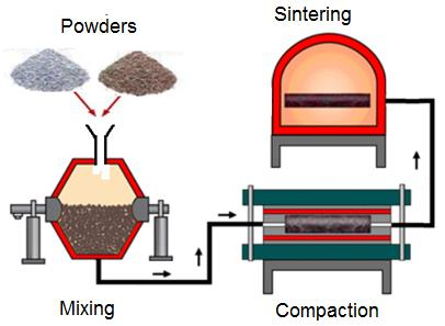
The copper sputtering target is a kind of copper product made of the metal copper, and it is used in the sputter coating to produce copper thin film. Simply speaking, there are two methods to make copper sputtering target from metal copper.
Casting: melt the raw material of a certain distribution ratio, pour the alloy solution into a mold to form an ingot, and finally machine it to become a sputtering target. The method is smelted and cast in a vacuum.
Powder metallurgy: melt the raw material of a certain distribution ratio, cast it into an ingot and then pulverize it, isostatically press the powder, and then sintering it at a high temperature to finally form a target.
Purity: Purity has a great influence on the performance of the film produced by sputter coating. Taking copper target as an example, the higher the purity is, the better the corrosion resistance and electrical and optical properties of the sputtered film are.
Impurity content: The impurities in the solid of the target material and the oxygen and water vapor in the stoma are the main pollution sources of the deposition film. Targets for different applications have different requirements of their impurity contents.
Density: The density of the target not only affects the sputtering rate but also affects the electrical and optical properties of the film. Thus, in order to reduce pores in the solids of the target and improve the properties of the sputtered film, the target is usually required to have a higher density.
Grain size and grain size distribution: For the same target, the sputtering rate of the fine-grained target is faster than that of the coarse-grained target; and the thickness of the target sputter-deposited film with a smaller difference in grain size (distributed uniformly) is more uniform.
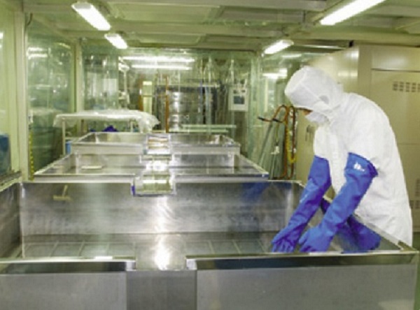
It is very important to keep the vacuum chamber clean. Residues formed during target sputtering collect moisture and other contaminants, directly affecting the success rate of vacuum coating. If the sputtering chamber is not clean enough, the sputter gun and the sputtering target will often short-circuit or exceed the target arc to discharge, filming surface roughness and chemical impurities. In addition to the vacuum chamber, the dark area shield, cavity walls and adjacent surfaces need to be kept clean. When cleaning the vacuum chamber, we recommend using a glass ball to blast the dirty parts, while using compressed air to remove spilled residue from the periphery of the cavity, and then gently polishing the surface with alumina impregnated sandpaper. After polishing, wash with alcohol, acetone and deionized water. It is recommended to use an industrial vacuum cleaner for auxiliary cleaning.
In addition, in order to ensure coating characteristics, it is also necessary to wash and dry the sputtering gas (argon or oxygen). After the substrate is placed in the sputtering chamber, air needs to be extracted to achieve the vacuum state required for the process.
When using the target, wear clean protective gloves and avoid direct contact with the target.
Target cleaning
The purpose of cleaning the sputtering target is to remove any dust or dirt that may be present on the target surface. Metal sputtering targets can be cleaned in four steps:
In the first step, the target is wiped with a soft, lint-free cloth soaked in acetone;
The second step is to clean the target with alcohol;
The third step is to wash the target with deionized water;
In the fourth step, the target was placed in an oven and dried at 100 degrees Celsius for 30 minutes.
For oxide ceramic sputtering targets, it is recommended to use a “langue-free cloth” for cleaning. After removing the contaminated area, the target is flushed with high pressure, low moisture argon to remove any contaminating particles that may create an arc in the sputtering system.
Target installation
During target installation, it is important to ensure a good thermal connection between the target and the stabilizing wall of the sputter gun. If the degree of warpage of the stave or backing plate is severe, the thermal conductivity of the target will be greatly affected, resulting in heat not being dissipated during the sputtering process, eventually leading to cracking of the target.
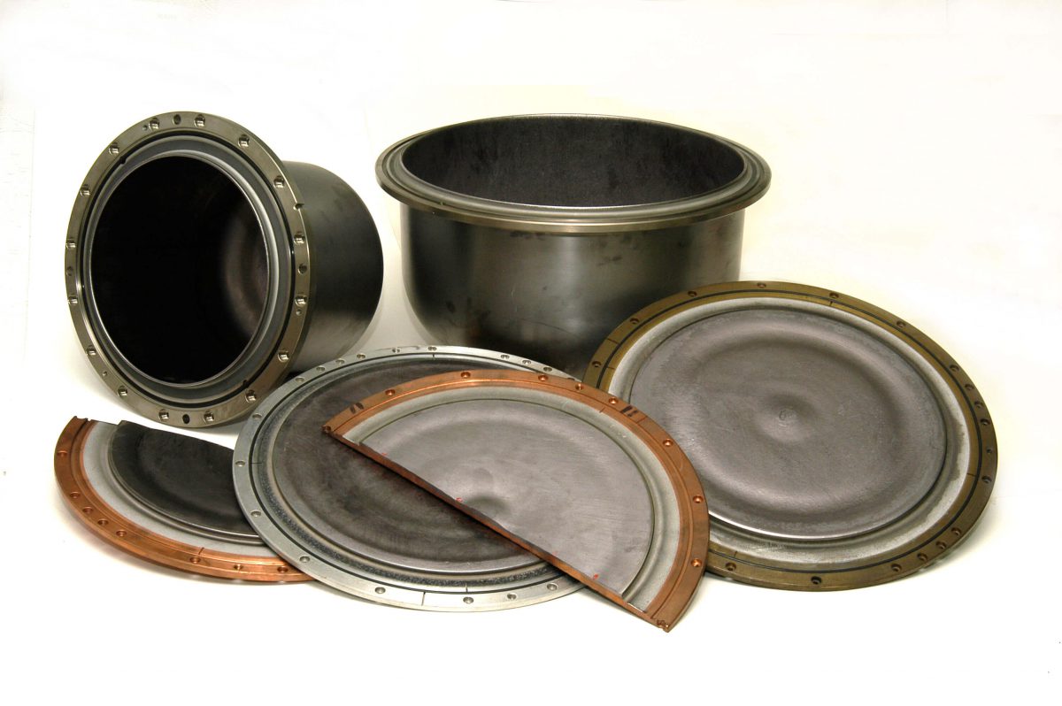
Target packaging and transportation
All targets should be packaged in a vacuum-sealed plastic bag with a moisture barrier. The outer packaging is usually a wooden box with an anti-collision layer around it to protect the target and rear targets from damage during transportation and storage.
In today’s electronics industry, many electronic components are manufactured using a vacuum coating process. Vacuum coating has become an indispensable technology for the manufacture of electronic components. The current vacuum coating technology is to evaporate and sputter a metal or alloy in a vacuum to deposit it on a substrate. Vacuum evaporation and magnetron sputtering coating are two main vacuum coating technologies.
Vacuum evaporation
History
In 1857, Michael Faraday first proposed the basic principle of vacuum evaporation. Later, in the 1930s, the oil diffusion vacuum pump was put into practical use, and it was mainly used to make the lens anti-reflection film. During the Second World War, the demand for materials from other optical machines increased, and vacuum evaporation also developed rapidly.
Principle
In a vacuum state, the evaporation pellets in the evaporation vessel is heated to cause atoms or molecules to escape and deposit on the surface of the evaporation material to form a solid film. Depending on the type of vapor deposition material or substrate, it can be classified into heating methods such as resistance heating, electron beam, high-cycle induction, and laser. The vapor deposition materials include metal evaporation materials such as aluminum, lead, gold, silver, platinum, and nickel, and materials capable of producing optical properties, and oxides and fluorides such as SiO2, TiO2, ZrO2, and MgF2 are mainly used. In addition to metal, vapor deposition can be used for resin and glass, and in recent years, continuous paper has also become vapor-depositable.
Advantages
The device is simple and easy to operate; the film formation rate is fast and the efficiency is high.
Disadvantages
The thickness uniformity of the film is not easy to control, the evaporation container has hidden dangers, the process repeatability is not good, and the adhesion is not high.
Magnetron sputtering coating
History
As a very effective thin film deposition method, magnetron sputtering technology has been widely and successfully applied in many fields, especially in the fields of microelectronics, optical films and material surface treatment, for thin film deposition and surface coating preparation. In 1852, Grove first described the physical phenomenon of sputtering. In the 1940s, sputtering technology began to be applied and developed as a deposition coating method. With the rapid rise of the semiconductor industry in the 1960s, this technology was widely used and widely used in the integrated circuit production process for depositing metal electrode layers of transistors in integrated circuits. The emergence and development of magnetron sputtering technology, and the use of reflective layers for CD production in the 1980s, the field of application of magnetron sputtering technology has been greatly expanded, and gradually become a common means of manufacturing many products, and in the last ten years, a series of new sputtering techniques were developed.
Principle
Electrons accelerate to the substrate under the action of an electric field. In this process, electrons collide with argon atoms to ionize a large amount of argon ions and electrons. Under the action of an electric field, argon ions accelerate the bombardment of the sputtering target, and sputter a large number of target atoms, and the target atoms are deposited on the surface of the substrate to form a film.
Advantages
The process repeatability is good, the film has high purity, uniform film thickness and good adhesion.
Disadvantages
The structure of the device is complicated, and once the sputtering target penetrates, the entire target is scrapped, so the utilization rate of the target is low. Using rotatory sputtering target can increase the utilization of the target.
Sputter coater targets have high requirements during use, requiring not only purity, size, and even grain size uniformity. These high requirements make us pay more attention when using sputtering targets. Let’s take a look at the five points of use of the sputtering coater target during use.
Sputter preparation
It is very important to keep the vacuum chamber and the sputtering system clean. Any residue formed by lubricating oil and dust, as well as pre-coating, will accumulate moisture and other contaminants, directly increasing the possibility of film failure. Apart from it, the unclean sputtering chambers, sputter guns, and sputtering targets will also cause system short circuits, target arcing and rough surface formation.
In order to maintain the composition characteristics of the coating, the sputtering gas (argon or oxygen) must be cleaned and dried. After the substrate is placed in the sputtering chamber, the air needs to be extracted to achieve the vacuum level required by the process.
Target cleaning
The purpose of target cleaning is the same as the first point in order to remove dust or dirt that may be present on the surface of the target and keep it clean.
Target installation
The most important precaution during target installation is to ensure a good thermal connection between the target and the stabilizing wall of the sputter gun. If the warp of the cooling stave or backing plate is severe, it may cause cracking or bending of the target during installation. In this way, the thermal conductivity of the backing plate to the target is greatly affected, resulting in the inability to dissipate heat during the sputtering process, which eventually causes the target to crack or off.
Short circuit and seal check
After the target is installed in the sputtering machine, it is necessary to inspect the circuit condition and seal of the cathode. It is recommended to judge whether there is a short circuit in the cathode by observing the way the resistance meter shakes. After determining that there is no short circuit in the cathode, water can be passed to the cathode to determine if there is water leakage.
Target pre-sputtering
It is recommended to use pure argon for target pre-sputtering, which can help clean the surface of the target. When the sputter coating target is pre-sputtered, it is recommended to increase the sputtering power slowly. The power-increasing rate of the ceramic target is recommended to be 1.5 Wh/cm2, and the pre-sputtering speed of the metal sputter coater target materials can be 1.8 Wh/cm2 with a reasonable power increase rate compared to the ceramic target block.
Stanford Advanced Materials (SAM) is a global supplier of a series of pure metals, alloys, ceramics and minerals such as oxides, chlorides, sulfides, oxysalts, etc. SAM Sputter Targets is a division of Stanford Advanced Materials, which specializes in manufacturing vacuum coating materials such as sputtering targets and evaporating pellets.
History of SAM
Stanford Advanced Materials was founded in 1994 and now has a history of 25 years.
SAM initially began supplying high-quality rare earth products to assist our customers in research and development (R&D). To meet the growing demand for rare earth products and other materials, SAM now offers sputtering materials not only for our R&D customers but also for manufacturers in the ceramics, metallurgical and electronics industries.
SAM supplies technology-grade materials to the industry and provides research institutions with high-purity chemicals (up to 99.99999%).
Products of SAM
SAM Sputter Targets is your reliable sputtering target manufacturer. SAM has long been committed to providing customers with high quality and reliable sputtering targets at very competitive prices.
Because we understand the importance of reliable and consistent materials to our customers’ R&D and production needs, we have established a strong relationship with our manufacturers.
By regularly visiting our manufacturers and talking to their management, production and quality control engineers and workers on the production line about the quality we seek, we have created truly effective partnerships. These valuable friendships built over the years have enabled us to deliver consistently high quality products to our global customers.
SAM’s motto is “We not only provide products, we also provide satisfactory service.” We believe that you will find SAM one of your favorite sputtering target suppliers.
For more information, you can contact us by email at target@samaterials.com or by calling (949) 407-8904. You can also visit our website at www.sputtertargets.net for information about our products, services, pricing and news.