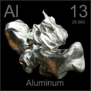
What is Copper Sulfide Sputtering target?

Copper sulfide is an inorganic compound with a chemical formula of CuS. It is dark brown and extremely insoluble. It is one of the most insoluble substances (second only to silver sulfide, mercury sulphide, palladium sulfide and platinous sulfide).

 Copper Sulfide Sputtering target
Copper Sulfide Sputtering target

Copper sulfide sputtering targets can be used in the semiconductor industry for the fabrication of thin film deposition from different materials for processing of integrated circuits, fabrication of architectural window glass used for energy conversation, data storage, hybrid or microelectronics, photonics  and fabrication of CDS as well as DVDs. Copper sulfide sputtering targets have different and new-fangled dimensions and product geometries.

Continue reading “What is Copper Sulfide Sputtering target?”

What is ITO (indium tin oxide) Sputtering Target?

As its name suggests, ITO sputtering target mainly contains three elements of indium, tin and oxygen. More specifically, ITO sputtering target is a black-gray ceramic semiconductor (as shown below) formed by a series of production processes after indium oxide and tin oxide powder are mixed in a certain ratio, and then sintered in a high temperature atmosphere (1600 degrees, oxygen sintering).

ITO

As one of the most widely used transparent conducting oxides, Indium tin oxide (ITO) has good electrical conductivity and optical transparency. The transmittance and resistance of ITO are controlled by the ratio of In2O3 to SnO2, respectively, and the performance is usually best when SnO2:In2O3=1:9. The most common method for preparing ITO films is physical vapor deposition (PVD). To know more information about PVD technology, please read this article What are the uses of PVD (Physical Vapor Deposition) coating. And, to know more about how to produce ITO target, please read another article Four main molding methods for ITO (Indium Tin Oxide) targets.

Continue reading “What is ITO (indium tin oxide) Sputtering Target?”

Working principles of a resistive touch screen and a capacitive touch screen

resistive touch screen and capacitive touch screenResistive screens and capacitive screens are the two main kinds of mobile screens on the market today. Generally speaking, resistive screen phones can be operated with a finger or a stylus; while capacitive screen phones can only be operated with fingers and cannot be operated with ordinary stylus, but we can use a dedicated capacitive screen stylus to substitute the finger to operate; while the resistive screen phone can be operated with a finger or a stylus. Why do they have such a difference? Is it related to their working principle? Let’s SAM Sputter Targets answer it for you.

Continue reading “Working principles of a resistive touch screen and a capacitive touch screen”

What is the difference between a capacitive screen and a resistive screen?

Mobile phones have become an indispensable part of contemporary society. You may use your mobile phone every day, but you don’t know about it. For example, the screens of a mobile phone are mainly divided into a resistive screen and a capacitive screen, but do you know the difference between these two kinds of screens? If you do not know the answer, let’s SAM Sputter Targets answer it for you.

screen

Simply speaking, capacitive screen phones can only be operated with fingers and cannot be operated with ordinary stylus, but we can use a dedicated capacitive screen stylus to substitute the finger to operate; while  resistive screen phones can be operated with a finger or a stylus. From this point of view, some people may think that the latter has an advantage. However, although the capacitive screen can only be operated with a finger, it can largely protect the screen and reduce false touches. Therefore, the two screens actually have their own advantages. Let’s then take a look at their strengths and weaknesses.

Continue reading “What is the difference between a capacitive screen and a resistive screen?”

Manufacturing process of semiconductor wafer

Semiconductor wafers are the basic material for manufacturing chips. The most important raw material for semiconductor integrated circuits is silicon, which is widely found in rocks and gravel in the form of silicate or silicon dioxide in nature. The manufacturing process of semiconductor wafers/silicon wafers can be divided into three basic steps: silicon purification, monocrystalline silicon growth, and wafer formation.

Silicon purification

The sandstone material is placed in a 2000 °C electric arc furnace which has a carbon source. At high temperatures, the silica in the carbon and in the sandstone undergoes a chemical reaction (carbon is combined with oxygen, leaving silicon) to obtain pure silicon having a purity of about 98%, also known as metallurgical grade silicon. Continue reading “Manufacturing process of semiconductor wafer”

Differences between vacuum evaporation and sputter coating

It is well known that vacuum coating has two common methods: vacuum evaporation and sputter coating. However, many people have doubts about the difference between evaporation and sputter coating. Let SAM Sputter Targets answer it for you.

sputter coating3First, let’s take a look at the definition of these two words. The vacuum evaporation is carried out by means of resistance heating, electron beam or laser bombardment in an environment with a vacuum of not less than 10-2 Pa, and the evaporation material is heated to a certain temperature to evaporate or sublimate a large number of molecules or atoms, and then directly deposited on a substrate to form a film. Continue reading “Differences between vacuum evaporation and sputter coating”

Five evaporation sources for heating

The evaporation source is a heating element used to vaporize  the molding material. The evaporation sources currently used mainly include the following types:

Resistance evaporation heating source

The resistance heating method is simple and easy to operate, and is a common application method: a filament-like or sheet-like high melting point metal (such as Tungsten, Molybdenum, Titanium, etc.) is made into an evaporation source of a suitable shape. It is equipped with an evaporation material to turn on the power supply, and the evaporation material is directly heated and evaporated. The resistance heating method should mainly consider two problems, the melting point and vapor pressure of the evaporation material; the reaction of the evaporation material with the coating material and the wettability caused by the coating material.

Electron beam evaporation source

The evaporation material is placed in a water-cooled copper dry pot and directly heated by an electron beam, which is called electron beam heating. It can vaporize the evaporation material and form a film on the surface of the substrate. It is an important heating method and development direction in the vacuum evaporation coating technology. In the resistance heating method, the coating material and the evaporation material are in direct contact, and the temperature of the evaporation material is higher than that of the coating material, and is easily mixed into the coating material, especially in the semiconductor device coating. Electron beam evaporation can overcome many shortcomings of general resistance heating evaporation, and is particularly suitable for preparing high melting point film materials and high purity film materials.

High frequency induction heating evaporation source

The high-frequency induction heating evaporation source places the graphite or quartz crucible containing the evaporation material in the center of the water-cooled high-frequency spiral coil, so that the evaporation material generates strong eddy current loss and hysteresis loss under the induction of the magnetic field in the high frequency band (to Ferromagnetic), causing the evaporating material to heat up until evaporation. The smaller the volume of the evaporated material is, the higher the frequency of induction is. In the large-scale vacuum aluminum plating equipment on the steel strip, the high-frequency induction heating evaporation process has achieved great success.

Radiant heating evaporation source

For materials with high absorption of infrared radiation, it can be evaporated by radiant heating, and many substances are evaporated by this method. In addition, the reflectivity of the metal for infrared radiation is high, and the absorption rate of quartz for infrared radiation is low, so they are difficult to be evaporated by radiation heating. The main advantage of the radiant heating method is that the evaporation is only heated on the surface, and the adsorbed gas is released on the surface without splashing the material.

Laser beam evaporation source

The evaporation technique using a laser beam evaporation source is an ideal film preparation method because the laser can be installed outside the vacuum chamber. This not only simplifies the space arrangement inside the vacuum chamber and reduces the abandonment of the heating source, but also completely avoids the contamination of the evaporation material by the evaporator, thus it is advantageous for obtaining a high-purity film.


Stanford Advanced Materials (SAM) Corporation is a global supplier of various sputtering targets such as metals, alloys, oxides, ceramic materials. If you are interested, please visit our website https://www.sputtertargets.net/ for more information.