Breast cancer, one of the major causes of deaths among women, affects about 12% of women around the world. According to research surveys, the smaller the breast cancer is when it is detected, the less the possibility of death. This requires that women should go over the medical body check regularly to decrease the risk of breast cancer. At present, molybdenum target mammography is considered the recommended breast screening examinations for women’s breast cancer.
What is the Breast Cancer?
Breast cancer is caused by the development of malignant cells in the breast. It is a sign of breast cancer when cells in the breast begin to grow out of control, and these cells usually result in forming a tumor.

Breast cancer itself is not a fatal disease because the breast is not an indispensable organ for maintaining human life. However, if the malignant cells spread to other important parts of the human body, such as the heart, the liver, and kidney, breast cancer may lead to death.
Breast cancer occurs almost entirely in women, but men can get breast cancer, too. And it is closely related to age—only 5% of all breast cancers occurring in women under 40 years old.
What is Molybdenum target mammography?
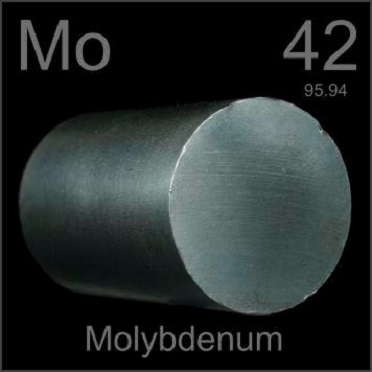
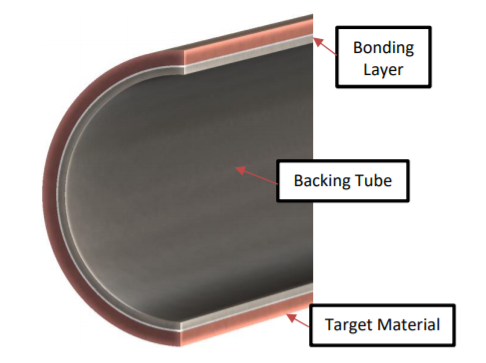
Molybdenum target, or molybdenum sputtering target, is known as the materials in physical vapor deposition for film coating.
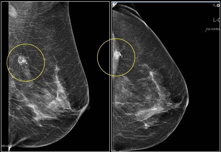
Molybdenum target mammography is another important application of Molybdenum target. It is a non-invasive method to test breast diseases such as breast mass and calcification. From the viewpoint of techniques, it is a digital imaging technology that combines traditional radiology technology with modern computer technology that transforms the X-ray image into a digital image that can be quantized. Molybdenum target mammography enables radiologists to find suspicious malignant lesions in mammography easier. Thus, it has been used as a routine examination to reduce the risk of breast cancer.
Why is Molybdenum target mammography beneficial?
Molybdenum target mammography is currently the primary choice for the diagnosis of breast disease. It is an easy and non-invasive method of examination which can accurately reflect the condition of the entire breast. What’s more, it can be used to observe the breast disease caused by various factors and the results are relatively reliable. With the help of Molybdenum inspection, some precancerous lesions can be found and can be followed up for observation. So it is beneficial for women’s health.
Above information is from SAM Sputter Target, a global sputtering targets manufacturer specialized in Molybdenum target.